How Japanese sensor manufacturing works comes down to a controlled pipeline: silicon wafers get coated with sensing films, patterned with photolithography, etched into microscopic structures, tested electrically, diced, packaged, and calibrated one part at a time before it ships. Japan’s part is process discipline, not exotic materials. The same sequence runs in fabs worldwide; what differs is how tightly contamination is controlled, how many quality gates sit between stations, and how relentlessly the line is improved after launch.
This guide walks the whole route, from the first specification a customer writes to the sealed part that goes into a robot arm, a car, or a medical cart. It also covers the parts that marketing pages leave out: stiction in MEMS release, drift in calibration, and the twelve to twenty-four month qualification cycles that decide whether a supplier is even in the running.
Table of Contents
- 1What Is Japanese Sensor Manufacturing?
- 2How Japanese Sensor Manufacturing Works From Design to Mass Production
- 3How Sensors Are Designed and Specified
- 4The specifications that decide the design
- 5Qualification gates before a supplier is even sampled
- 6Materials, Semiconductor Processes, and Packaging
- 7Silicon and the MEMS route
- 8What packaging decides
- 9Non-silicon materials
- 10Why Cleanroom Standards Decide the Outcome
- 11How Long Sensor Development Actually Takes
- 12Prototyping, Testing, and Quality Control
- 13Reliability tests a sensor has to pass
- 14Calibration and trim
- 15Statistical process control and quality gates
- 16How Japanese Companies Scale Sensor Production
- 17What high-mix low-volume asks of Japanese sensor production
- 18Where automation actually sits
- 19Why Japan’s Sensor Industry Matters
- 20The quality vocabulary, defined plainly
- 21The Main Challenges in Japanese Sensor Manufacturing
- 22Frequently Asked Questions
- 23What does Japanese sensor manufacturing include?
- 24Which types of sensors are manufactured in Japan?
- 25What is the role of MEMS in Japanese sensor production?
- 26How do Japanese manufacturers maintain sensor quality?
- 27Why are Japanese companies important in the global sensor market?
- 28Can small companies outsource sensor manufacturing in Japan?
- 29What to Understand First About Japan’s Sensor Industry
What Is Japanese Sensor Manufacturing?
Japanese sensor manufacturing is the design, fabrication, packaging and calibration of devices that turn a physical condition into an electrical signal a machine can read. Light, pressure, temperature, distance, sound, magnetism, humidity, acceleration. A sensor is the input layer of any automated system, so it also has to survive conditions the electronics around it would find unpleasant.
Not every sensor is semiconductor-based. Japan makes induction coils wound from copper, laser rangefinders, encoders with optical code discs, and thin-film chemical sensors. But the categories below cover most of what the country’s suppliers ship, and they split cleanly by how the physical quantity reaches the electronics.
| Sensor type | How it senses | Typical application |
|---|---|---|
| Proximity, inductive | Electromagnetic field disturbed by a metal target | Robot arm position, assembly-line presence detection |
| Photoelectric | Light beam interrupted, reflected or received | Part counting, colour and contrast inspection |
| MEMS pressure and inertial | Capacitive or piezoresistive change in a moving micro-structure | Tyre pressure, airbag triggering, accelerometers |
| CMOS image | Photodiodes on a shared silicon substrate | Machine vision, robotics, in-vehicle cameras |
| Magnetic and Hall | Magnetoresistive or Hall response to a magnetic field | Current sensing, position and angle sensing |
| Thermal and chemical | Resistance, catalytic reaction or optical absorption | Process lines, food and pharma, environmental monitoring |
The consumer electronics layer and the industrial layer are different businesses. A phone accelerometer is a commodity sold on volume and price. A pressure sensor certified for an engine bay has to hold its accuracy across minus forty to plus one hundred and twenty-five degrees, survive vibration for years, and stay traceable for a decade after the vehicle leaves the line.
How Japanese Sensor Manufacturing Works From Design to Mass Production
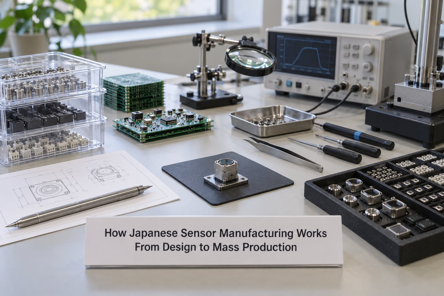
Sensor production is a repeatable sequence of about ten stages. The order matters less than the fact that each stage has an acceptance gate, and nothing moves forward until it passes. Here is the full route, from raw silicon to a sealed, calibrated part.
- Substrate preparation. The line starts with silicon wafers, either bought from a wafer maker or grown in-house. They get cleaned, thermally treated and inspected for crystal defects and surface particles. Everything built later inherits any flaw on this surface, so a rejected wafer here saves enormous cost downstream.
- Thin-film deposition. Sensing films go on next: metals, insulators, sacrificial layers, piezoelectric films. CVD grows films from gas, PVD sputters them off a target, and ALD lays down atomic layers for unusually tight thickness control. Deposition is the step where material purity matters most.
- Photolithography. A photosensitive resist is spun on, exposed through a mask or directly by a stepper, and developed. The mask is the pattern; the resist becomes a stencil saying which pixels of the wafer get etched or doped. Smaller features mean shorter wavelengths and more careful optics.
- Etching and structural formation. Wet etching dissolves exposed material in liquid. Reactive ion etching uses a plasma to cut vertically, giving sharper walls and far tighter tolerances. For a mechanical sensor, this is where a free-floating membrane or proof mass is actually carved out of solid silicon.
- Release and surface treatment. MEMS parts get a sacrificial layer dissolved so the moving element can finally move. Two problems bite here. Stiction, where the freed surface welds itself to the substrate from capillary force during drying, and afterwards, friction that slowly shifts the zero point. Anti-stiction coatings address both.
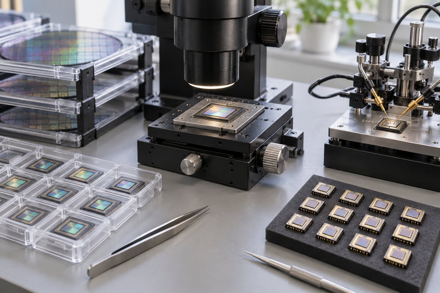
- Wafer-level test. Every die is probed while it is still on the wafer. Electrical tests screen for opens, shorts, leakage and reading out of range. Parts that fail here never reach packaging, which is what keeps the expensive downstream steps from working on bad sensors.
- Dicing. The wafer is cut into individual dies with a diamond blade or laser. This is a stress step. A bad cut cracks a part that had already passed every electrical test, so dicing parameters are tuned and monitored as closely as the fab steps.
- Die attach and interconnect. Each die is bonded to a lead frame, ceramic substrate or another die, then connected with wire bonds, flip-chip solder bumps, or through-silicon vias. Electrical tests run again on the packaged part, now measuring the assembled device rather than the raw die.
- Calibration and trim. This is the step that turns a working device into a measuring instrument. Each part is exposed to a known reference, its output is measured, and coefficients are burned into on-chip memory or stored for the host electronics. Without it, a part is roughly right; with it, a part is traceable and repeatable.
- Packaging and hermetic sealing. The final step closes the environment around the sensing element. A capacitive or resonant sensor changes behaviour as moisture enters, so many packages are welded or brazed hermetically in vacuum or inert gas. Others, like resistive pressure gauges, tolerate a vented cavity and use a hydrophobic membrane instead.
Packaging sometimes happens earlier. Wafer-level packaging seals devices while they are still on the wafer, which shrinks the part and cuts the amount of material each one consumes. Either way, the sequence above repeats many times, because a sensor is nearly always one small circuit among several inside a larger assembly.
How Sensors Are Designed and Specified
A sensor design starts with the measurement, not the circuit. What physical quantity, over what range, and how much error is tolerable? Everything after that question is trade-off arithmetic.
The specifications that decide the design
Accuracy and repeatability come first. Repeatability is how tightly consecutive readings agree; accuracy is how close the reading is to the true value. A sensor can be extremely repeatable and still read two percent high, which is fine for detecting presence and useless for dosing.
Response time matters when the thing being measured moves. A photoelectric sensor for a fast-moving conveyor and one for a slow pallet sit on a line differ mainly in this spec. Power consumption constrains battery and wireless designs, often forcing a trade between duty-cycle and resolution.
Environmental limits set the physical envelope: temperature extremes, humidity, vibration, shock, electromagnetic interference, and the media the part touches. Oil, coolant, detergent and food acids each attack different package materials in different ways. A part specified for a clean assembly line can fail in two years on a steel mill floor.
Package size is set by where it mounts, and mounting often decides the cost target. A die that fits a standard ceramic package is cheaper to make than one needing a custom cavity. A target cost per part at volume in the tens of thousands is a common reason to shrink a MEMS element rather than grow it.
Qualification gates before a supplier is even sampled
Automotive parts face the strictest entry requirements. AEC-Q100 grades parts by temperature and reliability testing. Functional safety under ISO 26262 applies to the sensing chain, not only the airbag controller. Industrial buyers add ingress protection ratings such as IP67 or IP69K, plus electromagnetic compliance testing to IEC 61000.
Those standards are why changing a supplier is slow. A new part is not just a new datasheet; it is a fresh qualification campaign, often with tooling, audit paperwork and a year of testing behind it.
Materials, Semiconductor Processes, and Packaging
Materials choice is the first fork in the road, and it decides which fabrication flow applies for the rest of the product’s life.
Silicon and the MEMS route
Silicon wins because it is abundant, its crystal lattice is near-perfect, and it carries the whole electronics ecosystem. MEMS takes this further: the same wafer carries mechanical structures and circuits, etched layer by layer. Pressure sensors, accelerometers, gyroscopes and microphones all follow this path.
Silicon is also the source of the hardest problems. Thermal drift shifts readings with temperature, and package stress after sealing can bend the membrane enough to move the zero point. Japanese makers have spent decades on polysilicon resistor trimming and on package designs where the die and the cavity are engineered as a single mechanical system.
What packaging decides
The package protects the sensing element, connects it electrically, and defines what the customer can do with it. Ceramic packages tolerate heat and harsh media and appear in automotive and industrial work. Metal cans and glass-die seals give tighter hermeticity for high-stability reference devices. Plastic moulding wins on cost and volume, and gets there by accepting more moisture over time.
Wafer-level packaging and through-silicon vias matter because size drives cost and power. Sealing on the wafer shrinks the footprint and reduces the material each sensor consumes, which matters enormously for a part shipped hundreds of millions of times into vehicles and wearables.
Non-silicon materials
Optical sensors need lenses and detectors that silicon cannot easily provide, so glass, polymer optics and compound semiconductors appear here. Chemical sensors rely on thin films that selectively absorb a gas or ion, which introduces drift from contamination and ageing. Magnetic sensors use amorphous metal ribbon, giant magnetoresistive films or Hall elements. Each brings material problems the fab operator has to manage differently.
Why Cleanroom Standards Decide the Outcome
Nothing on that ten-stage list survives a speck of dust. A single particle landing on a photoresist mask during lithography prints a defect onto every die on the wafer, and a particle landing on a released MEMS membrane can stop it moving entirely. Contamination control is therefore not housekeeping, it is a specification with a class number attached.
ISO 14644 defines cleanroom classes by particle concentration per cubic metre of air. The classes relevant to sensor work run from roughly ISO 5, where only a few thousand particles of 0.1 micrometres or larger per cubic metre are permitted, up to ISO 8 in assembly areas where the count runs into millions. Wafer processing typically runs dirtier than leading-edge logic fabs, but the MEMS and image sensor lines in Japan are clean enough that masking and metrology steps happen inside the same controlled envelope.
Three things hold a cleanroom steady. First, airflow: laminar flow ceilings push air across work surfaces in one direction so a particle cannot travel back to a sensitive step. Second, gowning and material handling: everything entering the room has been cleaned or extracted in an airlock, and wafers move in sealed carrier pods rather than by hand. Third, monitoring, which is continuous and automated. Particle counters sit in the ceiling and on the tools, and a step that drifts out of class stops rather than continuing to produce defects nobody will find until final test.
SEMI standards cover the equipment and materials side of the same problem, defining the specifications that toolmakers and material suppliers build to. ISO 14644 covers the room itself. Most buyers never see either document, but both explain why two factories running the same recipe can get different yield from the same product design.
How Long Sensor Development Actually Takes
The honest answer is that a simple sensor takes roughly a year, and an automotive one takes two to three.
A low-complexity sensor, say an inductive proximity probe, moves from specification to shipment in about nine to twelve months. Roughly a third of that is design and prototype, another third is qualification and pilot production, and the rest is ramp and logistics.
MEMS and image sensors take longer because the process has to be developed as well as the circuit. Realistic schedules run eighteen months to two years, and automotive programmes add a further qualification cycle with field data requirements that cannot be compressed. When a plant manager says a new sensor took two years, that is normally a literal description of the gate structure, not a failure to hurry.
Where the cost sits follows the same shape. Development spending concentrates on masks, tooling and the process recipe. Unit cost concentrates in wafer area, because a die is priced by the square millimetre it occupies. Shrinking a MEMS element by a fifth can cut the cost per part more than any negotiation, which is why design teams push footprint reduction as hard as they push accuracy.
Prototyping, Testing, and Quality Control
Prototype work runs on the same physics as production but none of the same economics. A handful of wafers go through an experimental line, the design gets iterated, and the process recipe gets written down well enough that someone else could repeat it.
Reliability tests a sensor has to pass
Environmental testing covers the range: thermal cycling, high and low temperature soak, humidity, and salt fog for marine and roadside work. Mechanical testing adds random vibration, mechanical shock, and drop testing. Switching endurance matters for any part with moving contacts, such as a reed or relay-style sensor.
Sensor-specific tests include one-sided or double-sided pressure loading for pressure gauges, and insulation resistance and high-voltage tests for magnetic current sensors. Zero-drift and offset checks catch parts whose calibration will wander in the field, which is the failure customers notice most.
Calibration and trim
Calibration happens on dedicated fixtures that expose parts to traceable references at several temperatures. Coefficients covering offset, span and non-linearity get stored on-chip or in the host controller, so the sensor reports a corrected value rather than a raw signal. Laser trimming of thin-film resistor networks handles the finest adjustments on high-accuracy parts.
The harder job is drift. A one-point correction taken at room temperature is worth less once the part spends a winter outside. Japanese makers invest heavily here, in reference devices that age predictably and in compensation schemes that hold accuracy across the full temperature range.
Statistical process control and quality gates
Every station feeds process data into statistical process control charts, where drift is flagged before it becomes a field failure. Wafer sort data, final test results and calibration residuals are tracked separately, and a shift in any of them pulls the line back for investigation.
The rules for reacting to an out-of-limit point come straight from jidoka, the idea of stopping the line the moment a defect appears instead of inspecting it downstream. Combined with poka-yoke, where a fixture physically cannot be loaded the wrong way, it changes how many defects ever reach a customer.
How Japanese Companies Scale Sensor Production
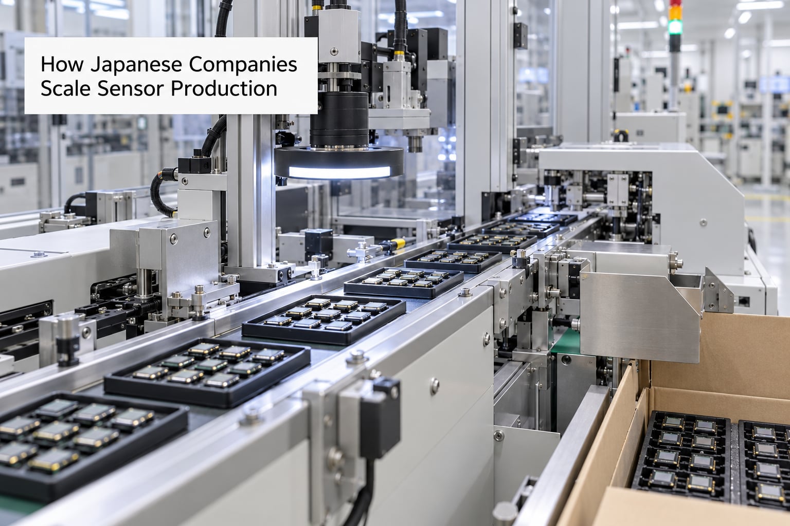
Samples are easy. Ten thousand good sensors a month is a different organisation problem, and ten million requires the process to be documented well enough that it survives being run by people who were not there when it was designed.
Scale-up usually follows a fixed order: stabilise the recipe, duplicate the tool set, train a second crew, then improve yield. Yield is the number that decides everything. Early in a product’s life it might sit in the seventies; mature automotive parts run well into the nineties after a team has spent months cutting defect density.
What high-mix low-volume asks of Japanese sensor production
Industrial sensors are made in dozens of variants with modest volumes each. Japanese factories handle this by standardising the back end: shared test platforms, parameter-driven calibration, and flexible assembly cells that change over between variants. Changeover time, not machine speed, is the metric that matters.
Just-in-time delivery to assembly lines runs the other way. Every part is traceable to its wafer lot, process recipe revision and calibration record, because a customer shipping cars needs to answer a question about a sensor built three years ago. That traceability requirement shapes the data systems, not just the paperwork.
Where automation actually sits
Automating a sensor fab is harder than automating an assembly line. Tools run long recipes with hundreds of parameters, and a fully autonomous line needs heavy process analytics to stay stable. Japanese factories automate widely but unevenly.
ABeam Consulting surveyed 6,186 Japanese manufacturing firms on smart factory progress and found only 32.9 percent actively pursuing initiatives, with 45.7 percent of those aiming at full automation. Only 15.7 percent were using digital twins. Where executives were engaged, 83.3 percent of efforts succeeded, against 16.7 percent when they were not. The gap is about attention, not technology.
Why Japan’s Sensor Industry Matters
Japan built a sensor industry by supplying hard industries rather than chasing the biggest consumer volumes. Automotive, industrial automation, robotics, energy and medical equipment all need parts that keep working for a decade in conditions that destroy ordinary electronics.
That customer base produced three things other regions had less reason to build: precision equipment makers that serve the whole region, a supplier base comfortable with small lots of customised parts, and factory operators who assume continuous improvement is part of the job rather than a special project.
The quality vocabulary, defined plainly
Kaizen means continuous improvement: small, constant, employee-driven changes rather than large campaigns. Monozukuri means the craft of making something, the accumulated skill that comes from doing the same task for decades. Genchi genbutsu means go and see, which in practice means an engineer stands on the line and watches the part instead of reading a report about the part.
Japan’s edge is process discipline rather than better raw materials, which is the conclusion practitioners working in these plants keep arriving at. The same silicon, the same gases, the same photoresist chemistry. What differs is how tightly the process is held.
The companies behind it are easy to name. Omron and Keyence dominate industrial factory sensing. Panasonic, Murata and TDK cover a huge range of MEMS, magnetic and component-level sensing. Denso is a major automotive sensor supplier in its own right. Sony Semiconductor Solutions makes the stacked CMOS image sensors used across cameras and vehicles.
The Main Challenges in Japanese Sensor Manufacturing
Precision is not free, and buyers should treat pricing as a signal rather than a surprise.
Japanese parts usually cost more than equivalent units from elsewhere. Some of that gap is labour and energy, some is amortised qualification and tooling, and some is simply margin. For a carmaker losing a wheel-speed sensor in a recall, the arithmetic is different from a hobbyist buying one.
Lead times stretch out for the same reason. A small-batch sensor that took a qualified process to produce cannot be switched to a different fab in a week. Lead times of twelve to twenty-four weeks are routine for industrial parts, longer when a line is ramping.
Capacity concentrates. Advanced MEMS and image sensor lines are few in number, so a single facility outage, earthquake or flood affects supply far more than the geographic spread of the assembly steps suggests. The 2011 earthquake and the automotive chip shortage of 2021 both made that concentration visible.
Miniaturisation keeps raising the cost of getting a part to work at all. Smaller features mean more demanding lithography, tighter contamination control, and harder yield problems. Calibration also gets harder as parts shrink, because a die takes up less physical space for the trim structures that correct it.
Currency and demand volatility add a commercial layer. A yen move changes landed cost quickly, and industrial demand swings with capital spending cycles. Suppliers that promised just-in-time volumes during an upcycle are the ones who struggle when orders halve.
Set against other manufacturing regions, the trade-off is fairly consistent. Japan spends heavily on process control and lands on higher unit cost with tighter tolerance bands. Taiwan and South Korea carry the highest volumes in semiconductor-adjacent work and compete hardest on cost at scale. Central and Eastern Europe compete on labour cost for assembly rather than on wafer processing. Germany and Switzerland compete on specific high-accuracy niches with engineering-led customisation.
| Factor | Japan | High-volume Asian fabs | Assembly-led regions |
|---|---|---|---|
| Relative unit cost | Higher | Lowest | Low |
| Tolerance consistency | Very tight, controlled process by process | Tight, optimised for volume | Set by the component spec |
| Typical lot size | Small to medium | Very large | Small to medium |
| Lead time | Often 12 to 24 weeks | Long in shortage, short otherwise | Moderate |
| Best fit | Harsh-environment, safety-critical, low-volume custom | Cost-sensitive high-volume consumer devices | Enclosures, cabling, secondary assembly |
Frequently Asked Questions
What does Japanese sensor manufacturing include?
It covers the full route from specification to sealed part: sensing material choice, wafer preparation, thin-film deposition, photolithography, etching, MEMS release and surface treatment, wafer-level test, dicing, die attach, calibration and hermetic packaging. Quality systems, reliability testing, yield management and production scale-up sit alongside those physical steps.
Which types of sensors are manufactured in Japan?
Japan supplies inductive and photoelectric proximity sensors, MEMS pressure and inertial sensors, CMOS image sensors, magnetic and Hall effect sensors, encoders, fibre-optic and laser sensors, and thin-film chemical sensors. The strongest areas are industrial factory sensing, automotive sensing and image sensors, where long service life and harsh-environment tolerance matter more than unit cost.
What is the role of MEMS in Japanese sensor production?
MEMS, or microelectromechanical systems, is the route behind most Japanese-made pressure sensors, accelerometers, gyroscopes and microphones. Mechanical structures are etched into silicon alongside circuitry, then released by dissolving a sacrificial layer. That release step brings two recurring problems: stiction during drying, and long-term friction that shifts the zero point.
How do Japanese manufacturers maintain sensor quality?
Quality comes from gates rather than inspection. Every process station has acceptance criteria tracked with statistical process control charts, and the line stops as soon as a reading drifts. The same ideas appear on the shop floor as jidoka, which halts production the moment a defect appears, and poka-yoke, which designs fixtures so a wrong action is physically impossible.
Why are Japanese companies important in the global sensor market?
Japan supplies a large share of advanced image sensors and industrial sensing, and it built its position serving automotive, robotics and energy customers that need parts to last a decade in extreme conditions. Japanese suppliers also co-develop sensors with their customers, so a new part is often designed around a specific machine rather than sold from a catalogue.
Can small companies outsource sensor manufacturing in Japan?
Yes, though usually through a supplier relationship rather than a direct fab deal. For a machined or wound sensor such as an inductive probe, a specialist contract manufacturer can build to your drawings in small batches. For MEMS or CMOS devices, the path runs through a chip design partner and a foundry, and the smallest realistic order quantities come with long lead times and NRE charges.
What to Understand First About Japan’s Sensor Industry
The single idea worth carrying away from how Japanese sensor manufacturing works is that the sensor is finished only when it is calibrated and sealed. The wafer steps get the attention in most explainers, but the package and the trim decide whether a part is a measuring instrument or a rough indicator.
Second, Japan’s advantage is procedural rather than material. The same silicon, the same gases and the same photoresist go into fabs everywhere. What differs is how tightly every station is held to specification, and how quickly a team returns to improve a process after it ships.
If you are evaluating a supplier, ask for the yield figure at the volume you plan to buy, the drift specification across temperature rather than a single-point accuracy, and the calibration record format. Those three answers tell you more than any brochure about precision.