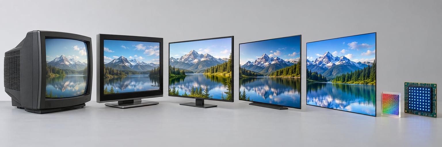
How Japanese display technology evolved is a story of mastering one screen technology at a time, then losing the factory economics of the next. Japanese engineers commercialised the colour cathode ray tube, the wall-mount LCD television, the first consumer OLED television and the small OLED panel, yet Japanese firms ended up making fewer large panels than South Korean and Chinese competitors.
The reason is not a lack of invention. It is the price of building fabs, and how quickly that price grew. Reading the arc from the 1960s to today explains why Japanese brands still lead in microdisplays, automotive screens and e-paper while handing large television panel production to Seoul and Chengdu.
Table of Contents
- 1How Japanese Display Technology Evolved: A Timeline
- 2Why Japan Became a Major Display Innovator
- 3How CRT and Plasma Established Japan’s Display Lead
- 4Why Trinitron CRTs lasted so long in studios and on desks
- 5How LCD Technology Became the Global Standard
- 6How LED-Backlit LCD Improved LCD Screens
- 7How Japanese Companies Advanced OLED
- 8Why large OLED panels were hard for Japanese TV makers
- 9How LCD Innovation Led to QD-OLED and MicroLED
- 10What Japan’s Display Evolution Means for Buyers Today
- 11Frequently Asked Questions
- 12Which display technology did Japan pioneer?
- 13Did Japanese companies invent OLED?
- 14Why did Japanese TV manufacturers struggle with large OLED panels?
- 15Is an OLED display always better than an LCD?
- 16What is the difference between QD-OLED and traditional OLED?
- 17What role did Japan play in developing microLED?
- 18Conclusion
How Japanese Display Technology Evolved: A Timeline
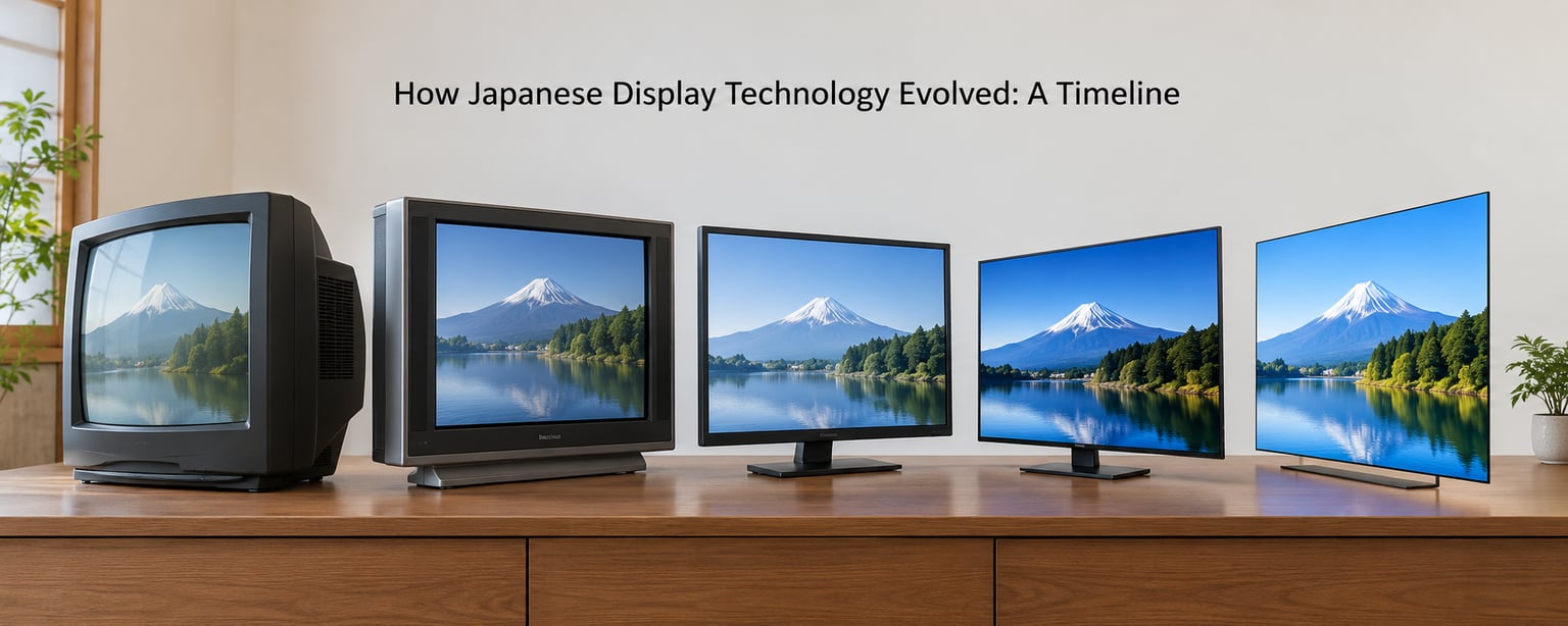
The table below traces how Japanese display technology evolved across five generations, naming the companies involved in each and the job each generation did in the living room.
| Era | Display family | Peak or development period | Representative Japanese companies | What it was used for |
|---|---|---|---|---|
| Broadcast era | Black-and-white CRT | 1950s to 1960s | Sony, Toshiba, Sharp, Matsushita | Living-room television and early computer monitors |
| Colour CRT | Trinitron aperture grille, shadow-mask tubes | Late 1960s to 1990s | Sony, Panasonic, NEC | Home television, broadcast monitors, colour-critical studio work |
| Flat panel | Plasma | 1990s to 2010s | Panasonic, Fujitsu, Hitachi | Large living-room screens where LCD was still dim |
| Flat panel | LCD, then TFT LCD, then LED-backlit LCD | 1990s to present | Sharp, Toshiba, Hitachi, NEC | Computers, phones, then nearly every television sold |
| Emissive | OLED, then QD-OLED and microLED research | 2000s onward | Sony, Sharp, JDI, Panasonic | Phones, cameras, high-end televisions, headsets, car screens |
Two threads run in parallel through those rows. The consumer panel thread moved from bulky tubes to flat rectangles, and each flat generation briefly belonged to Japan before Korea and then China took the volume end. The small-screen thread ran the opposite way: Japanese firms proved the emissive approach on handheld-sized glass, then struggled to make it cheap on television-sized glass.
Why Japan Became a Major Display Innovator
Japan’s display position started with broadcasting, not with gadgets. When television broadcasting began, the country built receivers from a standing electronics base of transformers, radio components and radio-frequency expertise, and a domestic market large enough to absorb early production runs.
Behind those factories sat an unusual concentration of suppliers. Japanese firms made their own glass, phosphors, liquid crystal materials, driver circuits and deposition equipment, so an engineer changing a screen recipe did not have to negotiate with an overseas vendor. That vertical integration shortened development loops in a way that showed up in product timing.
Television was also a national conversation about screen size. Families argued about room dimensions and diagonals, which pushed manufacturers toward bigger glass faster than in markets where the set was a minor piece of furniture. A larger screen meant more glass area per unit, which favoured whoever could hold yield on the biggest substrate.
Research culture reinforced all of it. Long-horizon corporate labs pursued display physics for decades rather than for the next product cycle, and the results were regularly published or standardised. Trinitron’s aperture grille, active-matrix driving and maskless deposition each came out of that kind of patient, unglamorous work.
How CRT and Plasma Established Japan’s Display Lead
Sony’s Trinitron, introduced in 1968, is still the clearest example of that lead. Most colour tubes used a shadow mask, a perforated metal sheet in front of the phosphor dots that blocked part of the beam and forced brightness reductions. Sony’s aperture grille replaced it with vertical wires, which left more beam open, reduced the dot pattern’s interference artefacts and made scan lines look cleaner on high-resolution sources.
The company got there through a failure worth remembering. Sony’s earlier Chromatron design used a wire grid stretched across the screen, and it demanded unstable voltages and delivered unreliable colour. The team kept the idea of a vertical aperture structure and threw away the wire-stretching mechanism, which is a decent summary of how most display progress actually happens.
Why Trinitron CRTs lasted so long in studios and on desks
Colour critical work resisted the flat-panel switch longer than most people expected. Broadcast monitors and desktop publishing screens valued stable geometry, no pixel grid at close viewing distance and predictable colour behaviour, and CRTs delivered those while flat panels were still catching up. Video designers, photographers and engineers kept Trinitrons in service well into the 2000s.
Collectors now chase that same equipment, and the second-hand market has become the way the era is measured in real money. A working professional broadcast monitor in good condition is worth far more than a home television of the same age, which is why the models people hunt for are the professional broadcast and computer monitor lines rather than the living-room sets.
Plasma took the other branch of flat-panel progress. Panels using ionized gas produced genuinely large screens in the late 1990s, with deep blacks and wide viewing angles that LCD panels of that era could not match, and Panasonic, Fujitsu and Hitachi built large businesses around them. Plasma lost on power consumption, thickness and the rising cost of the electronics behind the panel, and by the early 2010s it had been squeezed out of mainstream living rooms.
How LCD Technology Became the Global Standard
Liquid crystal display works by rotating the alignment of liquid crystal molecules with a voltage, which changes how much light passes through a polarising filter. That is a small change in optics, but it meant a screen could be flat, thin and light, because no vacuum tube and no gas chamber was involved.
The early limitation was that liquid crystal alone gave slow response and poor resolution. The change that mattered was putting a thin-film transistor, a tiny switch, on every pixel, so each one could be held at its own voltage. That active matrix let a display hold an image without refreshing it constantly, which is what made LCD usable for computer monitors and then for television.
Japanese companies pushed the manufacturing side hard. Sharp applied active-matrix work to LCDs earlier than most and moved through successive process generations to raise pixel density. The company’s own history records 1991 as the year it introduced the world’s first wall-mount LCD television, built on an 8.6-inch thin-film transistor panel with 437,760 pixels, and backed by a dedicated plant at Tenri and manufacturing capacity in the United States.
The bet was expensive and it required scale. Sharp, then Hitachi, then NEC and later Sony and Toshiba pooled their panel operations into Japan Display in 2012 with government support through the government-backed INCJ fund, betting that pooling would produce the fabs none of them could fund alone. The cluster around Osaka Bay, later known as Panel Bay, was the physical centre of that ambition, with major plants at Kameyama, Amagasaki, Tenri, Mobara and Sakai.
The consolidation did not hold the ground. Japanese display manufacturing lost share steadily through the 2010s as South Korean and Chinese makers added larger capacity with lower cost structures, and the government-backed model was later described in Japanese business press as lacking the vision to price its way through a commodity downturn.
How LED-Backlit LCD Improved LCD Screens
LCD technology did not end when emissive screens arrived; it got better. Early colour LCD panels used cold cathode fluorescent lamps behind the panel for backlighting, and those lamps are bulky, power-hungry and warm to the touch. Replacing them with light-emitting diodes removed the lamp problem entirely, because a diode is small, efficient and cool.
Two arrangements emerged. Edge-lit panels push light from the panel edge through a light guide, which makes a very thin screen possible at some cost to brightness uniformity. Direct-lit arrays put the diodes behind the panel in zones, which handles local dimming and therefore high-contrast picture quality, at the cost of thickness.
Good LCD televisions remained commercially important well after OLED arrived, for a plain reason: a large bright screen built on an established supply chain costs less to make than a large emissive one, and the gap was measured in real money rather than preferences. Plenty of viewers never noticed the difference at normal living-room brightness.
How Japanese Companies Advanced OLED
In an OLED pixel the organic compound emits its own light, so there is no backlight, no colour filter and no liquid crystal layer. Each pixel can be switched off entirely, which is why OLED panels produce true black and a contrast ratio that LCD panels simply cannot reach. Japan’s contribution to OLED was large, and it began with small glass rather than large.
Early OLED work reached cameras and then phones, where the small panel area kept evaporation yield manageable and where power consumption mattered enough to justify a new display architecture. Sony demonstrated the first OLED television, the 11-inch XEL-1, in 2007 and sold it as a prototype at a price that kept it out of homes, but the demonstration did exactly what a demonstration is meant to do: show that the approach worked at television scale.
The manufacturing problem was the fine metal mask. Producing OLED by evaporation means depositing organic material through a shadow mask with tiny openings, and the standard approach leaves an aperture ratio near 28 percent, meaning most organic material lands where it cannot be used. The mask itself is hard to make accurately at television size and hard to align. This is the constraint that pushed Japan’s research toward alternatives.
Why large OLED panels were hard for Japanese TV makers
The economics inverted for large displays. A fabrication plant is fixed cost spread across the substrate it processes, and Japanese companies attempting large OLED faced the worst version of that problem: the plant was built for a Japanese market of television buyers who were not willing to pay the premium, while the companies with the largest investment capacity were building the same panels in Korea and China.
Several different attempts followed. Pioneer worked on laser-assisted transfer. Sony and Panasonic, after winding down their own panel efforts, put money into JOLED, which developed a maskless approach now called eLEAP, depositing material through lithography rather than a shadow mask, with an aperture ratio around 60 percent and far more material landing on the pixel. Japan Display’s late-2023 acquisition of JOLED’s research operation kept that process alive inside a smaller company.
Japan Display itself never became the display champion the merger was meant to create. After nine consecutive loss-making years since its 2014 listing, a Taiwan- and China-linked consortium took control in 2019, a transaction widely read as the end of a state-directed attempt to build a national panel champion.
How LCD Innovation Led to QD-OLED and MicroLED
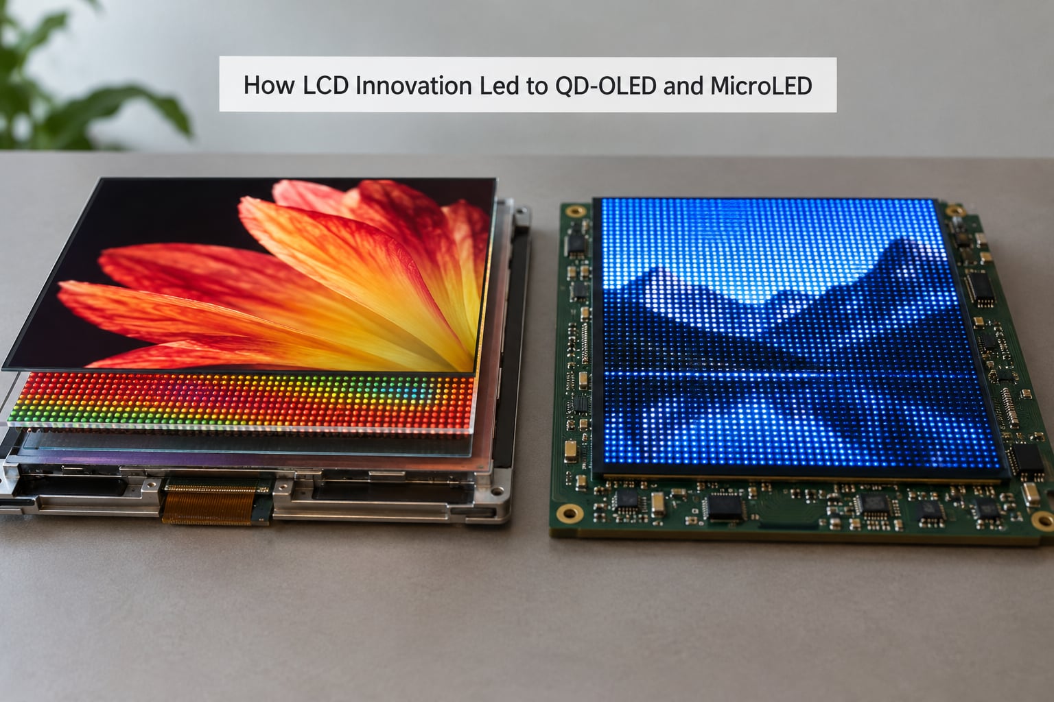
The same research threads that built Japan’s LCD and OLED capability fed the generations after them. Colour filter work, blue emitter development, backlight engineering and pixel packaging all matured alongside the main line rather than replacing it, and those threads surface in three newer formats.
Quantum dots are the first. A quantum dot is a tiny semiconductor crystal whose emitted colour depends on its size, so a layer of differently sized dots placed in front of a blue or white source can act as a precise colour converter with better colour saturation than a traditional dye filter. Sony commercialised this as QD-OLED, combining a quantum-dot colour layer with an OLED matrix, and helped move the format into consumer televisions. Traditional LCD makers put quantum dots into the backlight of an LCD instead, which is the source of the QD-LED and QLED naming confusion in shop displays.
MicroLED is the second. A microLED pixel is an inorganic LED small enough to serve as a single pixel, mounted on a backlight-free circuit board. Japanese firms have worked on the hard parts: blue LED efficiency, since blue remains the hardest colour to make efficient, mass transfer of millions of tiny dies onto a panel, and defect repair. Sharp, Panasonic, Sony and others have announced programmes and prototypes, while the format has stayed expensive because the transfer step is unsolved at scale.
The third thread is packaging rather than materials. Folding phones needed flexible glass and bendable pixel layouts, and Japanese suppliers provided both, which is one reason Japanese display capability keeps surfacing in products assembled elsewhere.
What Japan’s Display Evolution Means for Buyers Today
Reading a display label after sixty years of this history is easier once you treat each format as a set of strengths rather than a ranking. The table below gives the practical trade-off for the four formats a buyer will actually encounter.
| Format | Strength | Weakness | Suits |
|---|---|---|---|
| LCD, LED-backlit | Bright, cheap at large sizes, very long service life | Black level is a dark grey rather than true black | Daylit living rooms, bright offices, mixed content |
| OLED | True black, wide viewing angles, fast pixel response | Image retention over years of static content | Movie and series watching in a dim room, games |
| QD-OLED | OLED blacks with a wider colour gamut and a brighter panel | Costs more than an LCD of similar size | Colour-critical viewing and mixed bright-room use |
| MicroLED | Self-emissive with high brightness and no burn-in | High cost, with few models sold at consumer sizes | Command displays and very bright rooms |
Two more factors sit behind the panel choice. Resolution and pixel density decide whether text looks sharp at your desk or couch distance, and high-refresh capability decides how a game feels far more than the difference between two premium panels. Buy the panel that suits the room first, then the refresh rate.
It is also worth remembering where Japanese capability went. Microdisplays for headsets, high-temperature-tolerant automotive panels, e-paper, and the materials chemistry that feeds every OLED supply chain on earth are all places where Japanese engineering is still doing the difficult part.
Frequently Asked Questions
Which display technology did Japan pioneer?
Japan commercialised several display technologies before anyone else: the colour cathode ray tube and Sony’s Trinitron aperture grille from the late 1960s, the first wall-mount LCD television in 1991 from Sharp, the first OLED television in 2007 from Sony, and practical maskless OLED deposition now known as eLEAP. Japan’s record is strongest on getting a new screen type into a shipping product, weaker on keeping the manufacturing at large scale.
Did Japanese companies invent OLED?
No single company invented OLED, but Japanese firms were among the first to build it into shipping products. Early demonstrations came in the 1990s, and small OLED panels reached cameras and mobile phones before large panels became practical. Sony showed the first OLED television in 2007, and JOLED, backed by Sony and Panasonic, developed the maskless eLEAP process that avoids the shadow-mask limitation of early production.
Why did Japanese TV manufacturers struggle with large OLED panels?
The core problem was cost, not physics. Japanese television makers had the technology but not the matching market. Plant costs scaled with substrate area, domestic buyers were reluctant to pay a premium over an already good LCD, and the companies able to fund the largest lines were building them in Korea and China. A government-backed merger of Hitachi, Toshiba and Sony panel operations created Japan Display in 2012, but it was sold to a Taiwan and China-linked consortium in 2019 after nine loss-making years.
Is an OLED display always better than an LCD?
No. OLED wins on true black, wide viewing angles and pixel response, which matters most in a dim room for film and series. LCD wins on brightness in a daylit room, on price at large sizes and on long-term resistance to image retention. Many viewers watching mixed content in a bright room will find a good LED-backlit LCD entirely satisfying. Match the panel to the room and the content, not to a spec sheet ranking.
What is the difference between QD-OLED and traditional OLED?
Both are self-emissive panels that switch off individual pixels. QD-OLED replaces the traditional colour filter with a layer of quantum dots, tiny semiconductor crystals that emit a precise colour depending on their size. Because more of the emitted light reaches the viewer, the result is a wider colour gamut and higher brightness than a conventional OLED. Sony helped commercialise the format, while other brands use quantum dots in the backlight of an LCD instead, which is a different thing.
What role did Japan play in developing microLED?
Japan has been active in microLED research and has announced development programmes and prototypes, but the format is still expensive because the unsolved step is mass transfer: placing millions of tiny LED dies onto a panel at acceptable cost and yield. Japanese firms have contributed research on blue LED efficiency, transfer processes and defect repair, yet Korean and Chinese manufacturers have reached commercial microLED products first. Japanese capability in the field sits more in microdisplays for headsets than in large panels.
Conclusion
How Japanese display technology evolved is best read as iterative engineering rather than a series of breakthroughs and losses. Japanese teams kept the aperture grille idea from a failed Chromatron design, kept active-matrix driving from early LCD research, and kept deposition know-how from small OLED panels, then carried all of it forward into quantum-dot colour layers and maskless deposition.
What changed was not the science but the bill. Each generation needed more capital per line of production, and the countries that could fund the biggest lines took the volume. So start by matching the format to the room: LED-backlit LCD for bright rooms and large sizes, OLED for dark-room viewing and games, QD-OLED when colour range matters as much as black level.