Japan dominates photoresist supply because advanced resist chemistry is a decades-long accumulation of know-how, not a raw-material advantage. Japanese firms hold roughly 70% or more of the global photoresist market and around 95% of EUV resist, the most advanced type, according to an industry briefing published in April 2026.
Most people meet photoresist without knowing it. It is the liquid that gets spin-coated onto a silicon wafer, flashed with light through a mask, and turned into the microscopic stencil that becomes a chip’s circuitry. Without it, no fab in the world can pattern a transistor.
So the honest question is not whether the material matters. It is why one country ended up supplying so much of it, and why rivals have struggled to catch up despite enormous spending.
The short answer sits in five points:
- Purity is a physical wall. A contaminant measured in parts per billion can ruin an entire batch, and suppliers are held to defect counts that take decades of process discipline to hit.
- Every lithography generation resets the field. Moving from g-line to ArF to EUV means a new resist chemistry, which re-opens the competition and lets the incumbent leaders re-qualify first.
- Qualification cycles are long. A fab that validates a resist does not swap it lightly, so incumbency compounds.
- The market is small and grows slowly. Total industry sales were about 1.3 billion USD in 2018, growing under 8% in a year, according to Fuji Keizai. That is not an attractive market for a newcomer rebuilding from zero.
- The supplier base sits inside Japan’s own industrial cluster. Chemical makers, equipment vendors, research institutes and new fabs are all close enough to iterate together.
Last updated: October 2026
Table of Contents
- 1Why Japan Dominates Photoresist Supply
- 2What Is Photoresist and Where Is It Used?
- 3How the pattern actually gets onto the wafer
- 4What Gives Japan’s Suppliers a Technical Advantage?
- 5How purity and formulation explain why Japan dominates photoresist supply
- 6The resist generations, and why each transition matters
- 7What the market share numbers actually measure
- 8How Does Japan’s Supplier Ecosystem Reinforce Its Lead?
- 9How Important Are Scale, Quality Control, and Customer Trust?
- 10How Do Government Policy and Semiconductor Strategy Help?
- 11Why Does Japan Dominate Photoresist Supply?
- 12Can Japan Lose Its Lead?
- 13Frequently Asked Questions
- 14Does Japan supply all of the world’s semiconductor photoresist?
- 15Which companies are major suppliers of semiconductor photoresist in Japan?
- 16Why is it difficult for chipmakers to switch photoresist suppliers?
- 17Does every semiconductor made in Japan use Japanese photoresist?
- 18What could weaken Japan’s position in the global photoresist market?
- 19What Should Readers Take Away First?
Why Japan Dominates Photoresist Supply
Japan leads because the advantage sits in accumulated process know-how, specialist suppliers, quality infrastructure and tight integration with chipmakers, not in raw materials. The strength concentrates in high-purity, advanced photoresists for semiconductor manufacturing, which is where the demanding customers and the tightest defect budgets sit.
It is worth separating two things people often blur together. There is a broad market of photoresist, including the simpler formulations used for printed circuit boards and display panels, and there is the narrow, fast-moving market for semiconductor-grade resist at advanced nodes. Japan’s share looks very different depending on which one you measure, and most of the headline numbers floating around online refer to the second.
What Is Photoresist and Where Is It Used?
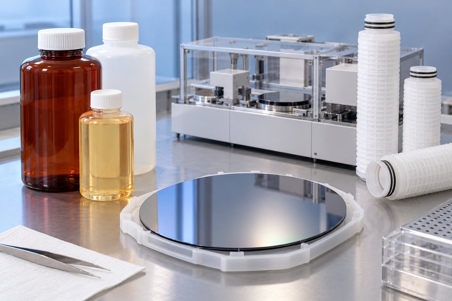
A photoresist is a light-sensitive liquid polymer. A machine called a spin coater spreads it across a silicon wafer in a film a few hundred nanometres thick, then a mask projects light through it. Where the light hits, the resist’s chemistry changes and becomes soluble in developer; where it misses, it stays put.
The result is a pattern. That pattern is then used as a stencil for etching, deposition and ion implantation, and each round of it builds one more layer of circuitry on the same piece of silicon.
How the pattern actually gets onto the wafer
- Coat. The resist liquid is spun onto the wafer; a solvent evaporates and leaves a uniform film.
- Expose. A reticle, or mask, projects light through the lithography tool. Shorter wavelengths print smaller features.
- Develop. Developer removes the exposed (or unexposed, depending on chemistry) parts, leaving the pattern.
- Etch and deposit. The pattern is transferred into the layers below, then stripped and repeated for the next layer.
- Inspect. Defects are measured and fed back into process control.
Semiconductor-grade resist is made to much tighter specifications than the kind used in printed circuit boards or LCD panel production. Panel makers buy larger volumes with looser defect budgets; semiconductor fabs buy smaller volumes with near-zero tolerance. Japan’s dominance sits overwhelmingly in the second category.
What Gives Japan’s Suppliers a Technical Advantage?
The advantage comes down to chemistry, purification, defect control, formulation expertise and a validation record that competitors have to match one customer at a time. Four Japanese names dominate the advanced end: Shin-Etsu Chemical, Tokyo Ohka Kogyo, JSR and Fujifilm Electronic Materials, with Sumitomo and the American firm DuPont also holding meaningful positions.
How purity and formulation explain why Japan dominates photoresist supply
The physics is unforgiving. A single particle left in the resist film becomes a defect in the finished pattern, and one defect in the wrong place can kill a chip. Tokyo Ohka Kogyo has illustrated the standard with a memorable image: a single drop of coffee in two Olympic-sized swimming pools of liquid would be an unacceptable contamination level. JSR has used a similar one, comparing a few tainted golf balls to spoiling a production batch the size of Japan.
Those analogies are not marketing fluff. They describe a supply chain where raw polymer has to be purified, formulated, filtered, packaged and shipped under conditions that do not introduce new contamination. Getting there takes facilities, metrology, cleanroom discipline and a trained workforce that has been doing the same thing for a long time.
The resist generations, and why each transition matters
Every time the industry moves to a shorter wavelength, the resist has to be redesigned. That is the recurring mechanism that keeps renewing Japan’s position: incumbents have the formulation library and the customer relationships to qualify first, while newcomers start from a blank page.
| Generation | Light source | Typical node | Era |
|---|---|---|---|
| g-line, h-line, i-line | 436 nm, 405 nm, 365 nm | Above 500 nm, legacy nodes | 1980s through the 1990s |
| KrF | 248 nm | around 130 nm | Late 1990s onward |
| ArF dry | 193 nm | around 100 nm | Early 2000s onward |
| ArF immersion | 193 nm in liquid | 65 nm down to 45 nm | 2010s |
| EUV | 13.5 nm | 5 nm class and below | 2019 onward |
The generations blur in real production, because immersion and EUV overlap on the same product roadmaps. The useful takeaway is the direction of travel: shorter wavelengths, tighter requirements, more requalification.
What the market share numbers actually measure
You will see 50%, 70%, 72.5%, 87% and 95% quoted in different places. They are not contradictions. They measure different things in different years.
| Figure | What it measures | Source and year |
|---|---|---|
| Roughly 50% | Broad global photoresist market, all types | Semiconductor industry podcast, 2024 |
| About 70% and up | Global photoresist supply, general framing | Advanced materials briefing, April 2026 |
| 72.5% combined | JSR, Tokyo Ohka, Shin-Etsu and Fujifilm Electronic Materials together | 2021-2026 industry report |
| About 87% | Japanese and American companies combined | 2021-2026 industry report |
| About 95% | EUV resist only, the most advanced generation | Advanced materials briefing, April 2026 |
Shin-Etsu alone holds roughly 40% of the global ArF resist market, and Tokyo Ohka Kogyo is a top-three EUV supplier. That combination of company-level and generation-level data is the more useful picture than any single headline percentage.
How Does Japan’s Supplier Ecosystem Reinforce Its Lead?
A resist supplier is not a catalogue item. It sits inside a feedback loop with the fab that uses it, and Japan built that loop over decades. When a defect shows up on line three, the conversation between the resist engineer and the process engineer is short, direct and continuous.
Three things concentrate that loop. First, chemical producers sit near equipment makers, so a change in the coater or developer tool gets matched to a change in the resist. Second, research institutes and university groups have worked on resist chemistry for decades, feeding graduates and patents into industry. Third, new fab capacity keeps appearing nearby, giving suppliers immediate test sites.
The current build-out makes that visible. TSMC’s Kumamoto fab in southern Japan is supported by Sony and Denso investment, Micron is operating in Hiroshima, Samsung is building in Kumamoto, and Rapidus is developing 2 nm logic in Hokkaido. SK Hynix has also announced a memory fab in Miyagi. Every one of those plants needs qualified resist, and proximity shortens the qualification loop.
The same cluster shows up in the tool business. Tokyo Electron and SCREEN Holdings together hold a large share of coater and developer equipment, so the resist, the machine that applies it and the engineer who tunes it often sit within a few hours’ drive.
How Important Are Scale, Quality Control, and Customer Trust?
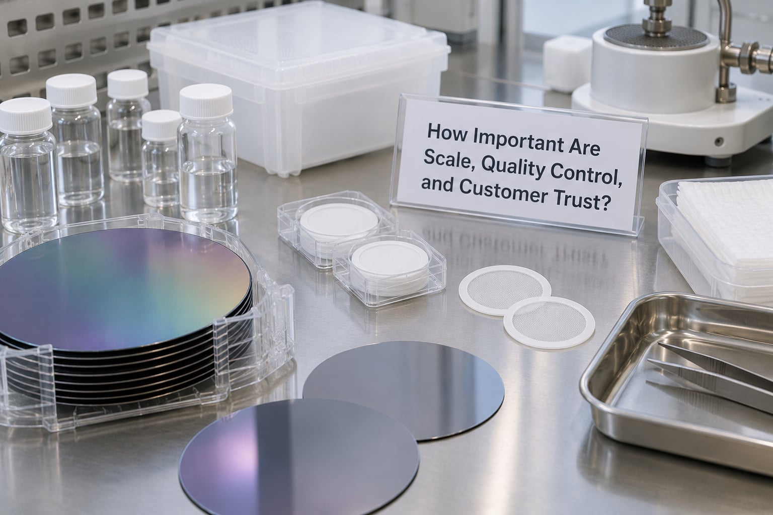
Scale matters less here than you would expect, because the volumes are small. The real constraint is consistency: a fab needs the same defect performance on the batch it receives next month as on the batch it qualified last quarter. That kind of batch-to-batch stability comes from process control, not from large plants.
Customer trust is the harder asset. Once a resist is validated in a production flow, changing it means re-qualifying from scratch: test wafers, exposure dose tuning, focus and overlay re-optimisation, defect inspection, and months of yield monitoring while output runs at reduced rates. A supplier that has completed that process at several leading-edge fabs holds something a laboratory cannot reproduce in a quarter.
The economists who study this position tend to reach the same conclusion. Rebuilding a competitive resist business would mean matching decades of R&D spending and then rebuilding the reputation, and because resist is consumed in modest volumes, the recovered revenue rarely justifies that outlay. That is the quiet barrier behind the whole industry.
How Do Government Policy and Semiconductor Strategy Help?
Policy reinforces the position rather than creating it. Japan’s export control system keeps a restriction list covering more than 25 semiconductor-related materials and components for designated destinations, which turns a supply position into diplomatic pressure. Separately, national industrial policy has supported domestic fab investment and materials capacity, and Japan’s semiconductor fabrication materials market was valued at about 6.8 billion USD in fiscal 2023 with forecasts approaching 10.9 billion USD by fiscal 2031.
There is a second, subtler policy effect: industrial subsidies to fabs create guaranteed demand for domestic materials suppliers, which lowers the risk of investing in a new resist line.
Still, state support is the amplifier, not the source. Subsidies can fund a plant; they cannot buy the formulation library, the defect history and the qualification relationships that take twenty years to accumulate. Any explanation of Japanese dominance that leads with government money has the causal order backwards.
Why Does Japan Dominate Photoresist Supply?
Eight factors account for the position, and they reinforce each other rather than standing alone. The practical significance column matters most, because it shows why each factor is hard to copy.
| # | Factor | Practical significance |
|---|---|---|
| 1 | Precursor chemicals and polymer supply | Consistent base resins and photoacid generators feed the formulation work |
| 2 | Formulation know-how | Balancing resolution, sensitivity and defect performance is the hard part |
| 3 | Production quality and clean handling | Parts-per-billion contamination control across the whole batch |
| 4 | Supplier relationships | Co-development with fabs turns into validated, hard-to-displace positions |
| 5 | Ecosystem density | Chemicals, equipment, institutes and new fabs all sit close together |
| 6 | Intellectual property | Decades of patents protect formulations that cannot be reverse-engineered from a sample |
| 7 | Long qualification cycles | Switching costs mean an installed supplier tends to stay installed |
| 8 | Small, slow-growing market | Weak incentives for anyone to fund a from-scratch challenger |
The historical thread behind these factors is worth tracing. JSR entered resist from tire rubber, a pivot driven by the decline of its core business and by Mitsubishi’s investment in it during the late 1980s. Tokyo Ohka Kogyo controlled as much as 90% of Japan’s domestic resist market by the mid-1980s. A joint research deal with IBM in 2000 helped push the industry into ArF-era chemistry just as the transition began.
Can Japan Lose Its Lead?
Yes, and it is worth being clear about the limits of the claim first. Japan does not supply all photoresist. DuPont is a major American supplier, Merck’s electronics business is significant in advanced chemistry, and Korean and Taiwanese producers serve their home markets. China has built real capability in the lower and middle tiers.
Against that, China’s domestic share of ArF resist remains in the low single digits, according to the April 2026 briefing. Its National IC Fund Phase II, sized at about 344 billion yen, explicitly prioritises photoresists and related core materials, so funding is not the constraint. Time is.
The risks to Japan’s position fall into a few groups. Concentration risk sits with a handful of firms; trouble at one supplier has direct consequences. Geopolitical risk cuts both ways, because Japan’s controls depend on cooperation with allied governments. Environmental and permitting constraints add years to new chemical capacity. And generational risk is real, as the engineers who hold the formulation knowledge retire, and written documentation rarely captures what a person knows about a filtration step.
There is also the sobering counter-history: the same countries that once dominated DRAM and LCD manufacturing lost those positions. Materials positions are more durable, but not permanent.
One last note on evidence quality. Reports that Japan has quietly restricted photoresist shipments to Chinese fabs have circulated widely and remain unverified in credible reporting. Treat them as market rumour until a supplier or government confirms them.
Frequently Asked Questions
Does Japan supply all of the world’s semiconductor photoresist?
No. Japanese firms hold roughly 50% to 70% or more of the broader global market depending on how the figure is scoped, and around 95% of EUV resist, the most advanced generation. DuPont is a major American supplier, and Korean, Taiwanese and Chinese producers serve their own markets. The smaller 50% figure covers all resist types; the 95% figure covers EUV only.
Which companies are major suppliers of semiconductor photoresist in Japan?
Four Japanese companies dominate advanced photoresist: Shin-Etsu Chemical, Tokyo Ohka Kogyo, JSR and Fujifilm Electronic Materials, which together held about 72.5% of the global market in a 2021-2026 industry report. Shin-Etsu alone holds roughly 40% of global ArF resist, and Tokyo Ohka Kogyo ranks among the top three EUV suppliers. Sumitomo also operates in the sector.
Why is it difficult for chipmakers to switch photoresist suppliers?
A validated resist is tied to a specific process flow. Swapping one means running test wafers, retuning exposure dose, focus and overlay, then monitoring yield for months while output runs below normal. Because resist volume is small and the qualification effort is large, most fabs stay with an approved supplier for years unless a new node forces a redesign.
Does every semiconductor made in Japan use Japanese photoresist?
No. A Japanese fab uses whatever resist its qualified process specifies, which is most often Japanese but not always. Fabs outside Japan run their own approved supplier lists, so where a plant sits says little about the material it buys. Conversely, chips made in Taiwan or Korea very often rely on Japanese resist. The material follows the process technology and its qualification history, not the country of assembly.
What could weaken Japan’s position in the global photoresist market?
The main pressures are a slow build-out of Chinese ArF capability funded by the 344 billion yen second phase of China’s national IC fund, plus subsidy-backed localisation efforts in South Korea, the United States and Europe. Concentration among a few Japanese suppliers, retirement of experienced engineers, environmental permitting delays and any shift in allied export-control cooperation could also erode the position over time.
What Should Readers Take Away First?
Start with the distinction everyone skips: basic resist versus advanced resist. Once you separate the broad market from the semiconductor-grade, EUV-era segment, the share numbers stop looking contradictory and the story gets much simpler.
Then treat Japanese dominance as a systems result rather than a single resource. Chemistry, purification, defect control, formulation libraries, qualification relationships and a dense industrial cluster reinforce each other, and no one of them is decisive on its own.
The practical implication for anyone tracking hardware is that a photoresist shortage would not be visible as a price move overnight. It would appear as fab qualification delays, slower capacity ramps and lead-time extensions, which is roughly how the 2019 Japan-Korea dispute played out, when Korean firms were reported to have depended on Japan for over 90% of their fluorinated polyimide and resists.