Japan builds very few of the world’s most advanced chips, yet a large share of the wafers, photoresists, photomasks, polishing slurries, gases and packaging films those chips are printed on come from Japanese factories. That is the japanese chip materials industry explained in one line: a cluster of specialist chemical and materials makers that sells to chip fabs in Taiwan, South Korea, the United States and Europe, and is now hard to replace because each material has to be qualified inside a customer’s production line before it is ever used.
The distinction matters, because headlines about Japan’s lost chip industry and headlines about Japan’s control of critical materials are both true and they describe different businesses. Fabrication is capital-intensive and geographically mobile. Materials chemistry is slow, messy and sticky. I spent a few weeks reading through supply-chain breakdowns and industry commentary to get the picture straight, and the mental model that finally worked for me was simple: a fab is a building full of machines, and Japan mostly sells the consumables that flow through them.
Below is the plain-language version, from silica to the packaged chip, with the segments that matter, the companies that illustrate them, the qualification rules that lock customers in, and the risks that could loosen that grip.
Table of Contents
- 1What Is the Japanese Chip Materials Industry?
- 2What these materials have in common
- 3Japanese Chip Materials Industry Explained: From Sand to Silicon
- 41. Industrial silicon and the wafer
- 52. Wafers for compound semiconductors
- 63. Photoresist and the auxiliary coatings
- 74. Photomask and mask blank
- 85. Gases and wet chemicals
- 96. Polishing and deposition materials
- 107. Substrates, films and packaging
- 118. The shipped chip
- 12What Are the Most Important Chip Materials?
- 13How Does Japan’s Chip Materials Supply Chain Work?
- 14Which Japanese Companies and Regions Matter Most?
- 15Why Is Japan Important Despite Limited Chip Fabrication?
- 16How Do Semiconductor Qualification and Quality Control Work?
- 17What Are the Main Risks to Japan’s Materials Industry?
- 18What Could Strengthen Japan’s Position in Chip Materials?
- 19How Should Investors and Tech Professionals Read Industry News?
- 20Frequently Asked Questions
- 21Is Japan a major semiconductor manufacturing country?
- 22What chip materials is Japan best known for supplying?
- 23Does Japan manufacture the silicon used in its semiconductor materials?
- 24How important are Japanese photoresists to chip production?
- 25Can Japan reduce its dependence on imported semiconductor materials?
- 26Conclusion
What Is the Japanese Chip Materials Industry?
The Japanese chip materials industry is the group of Japanese companies that supply the consumable inputs a semiconductor fab burns through to make chips: silicon wafers, photoresists, photomasks and mask blanks, electronic specialty gases, ultra-high-purity wet chemicals, CMP slurries and pads, sputtering targets, deposition precursors, circuit-board substrates and advanced packaging films.
None of these are finished products a consumer buys. They are process inputs, consumed continuously, measured in parts per trillion, and specified so tightly that changing one can change the yield of an entire production line.
Customers are the fabs themselves. A Japanese resist maker may ship from a plant in Yamaguchi to a fab in Hsinchu, Kumamoto, Dresden or Arizona, and the chip that comes out the other end sells as a phone, a server rack or a car. That is why the industry’s reach is far larger than Japan’s own chip output.
What these materials have in common
Four traits separate materials from the other parts of the supply chain. They are consumables rather than machines, so demand scales with wafers started rather than with fab count. They are specification-locked, so a customer who qualifies one resists rarely adds a second. They are chemically hard, so substitutes take years to reach production quality. And they are largely invisible in the finished product, which is exactly why shortages attract so little attention until a fab line stops.
Japanese Chip Materials Industry Explained: From Sand to Silicon
The production sequence below runs from raw input to packaged chip. It shows which materials arrive at a fab by delivery truck and which are transformed upstream, sometimes in the same country and sometimes abroad.
1. Industrial silicon and the wafer
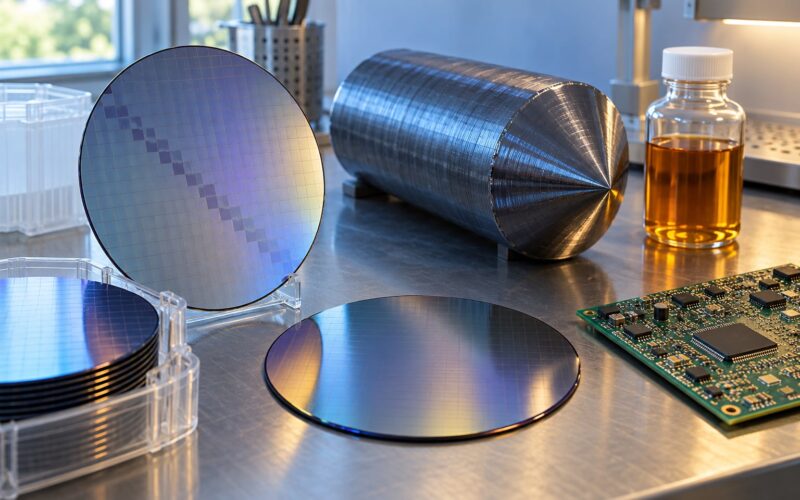
Quartz is reduced to metallurgical-grade silicon, then purified to semiconductor-grade polysilicon at nine or more nines of purity. The polysilicon is melted and pulled into ingots, which are sliced into thin discs, lapped, polished and inspected. The output is a 300mm silicon wafer, the substrate every chip is built on. In Japan this step is dominated by Shin-Etsu and SUMCO, with global share figures typically reported around half the 300mm market between the two leaders.
2. Wafers for compound semiconductors
Silicon carbide and gallium nitride substrates are grown in dedicated crystal facilities for power electronics and RF. This is a smaller, more specialised corner of the Japanese materials business, with domestic producers serving traction inverter and radio-frequency customers.
3. Photoresist and the auxiliary coatings
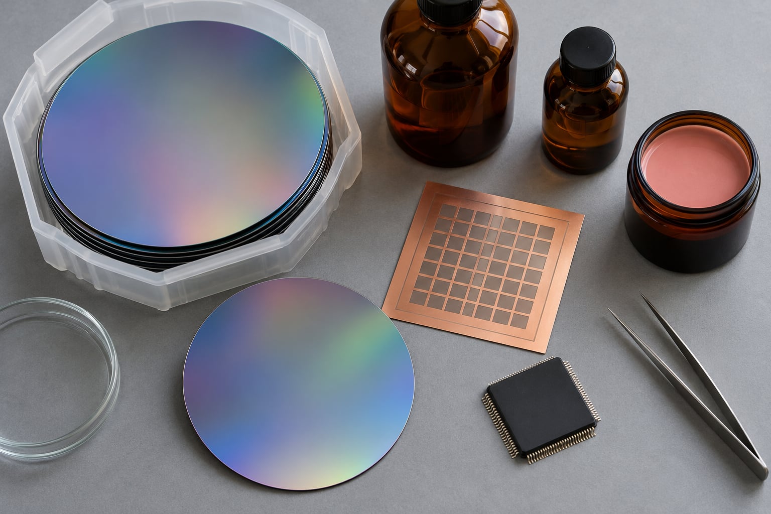
A photosensitive polymer is spun onto the wafer, baked, and later stripped away. The resist itself is only part of the chemistry: bottom anti-reflective coatings, top coatings, developers and an ever-growing list of process-specific additives sit alongside it. Japan has been described as holding roughly 90% or more of global photoresist supply in several published breakdowns, which is why the category draws the most attention and the most export-control speculation.
4. Photomask and mask blank
Patterns are written onto a mask that projects light onto the resist. The mask itself, plus the high-purity quartz blank it is etched from, is a separate supply chain from the resist. Japanese firms are widely credited with about half of advanced photomask supply, and mask blanks are a bottleneck that sits upstream of both.
5. Gases and wet chemicals
Etching, deposition, doping and cleaning consume specialty gases such as fluorine, silane and rare mixtures, plus wet chemicals at purities a laboratory reagent supplier would find absurd. These arrive in bulk, on dedicated supply systems, and are the easiest material category to see in a plant’s delivery schedule.
6. Polishing and deposition materials
CMP slurry and pads flatten each layer after deposition, which is what lets modern logic shrink. Sputtering targets and CVD or ALD precursors are the metals and molecules that become the wiring. CMP in particular is a segment that industry coverage tends to skip and that a materials specialist would put high on the list.
7. Substrates, films and packaging
Once the wafer is diced, chips need a package: a resin-based build-up film for high-end substrates, underfill, mould compound, and increasingly specialised films for chiplet and stacked designs. Ajinomoto’s ABF film, derived from a compound associated with a food additive, is the clearest example of a Japanese material quietly sitting inside nearly every high-end AI accelerator and server chip.
8. The shipped chip
That is the end of the materials chain. Assembly, test and system integration sit mostly outside Japanese material suppliers’ scope, though several of them sell directly into the same advanced packaging plants that are being built in Japan, Taiwan and Singapore.
What Are the Most Important Chip Materials?
This table compares the segments that actually gate advanced production. The share column reflects commonly cited industry estimates, and the figures differ between studies and years, so read them as order of magnitude rather than a census.
| Material | What it does | Typical use | Japanese industry role |
|---|---|---|---|
| Silicon wafers (300mm) | The substrate the whole circuit is built on | Logic, memory, analog | Two Japanese suppliers hold roughly half the 300mm market |
| Photoresist | Light-sensitive polymer that records the circuit pattern | Every lithography layer | Often cited at 90% or more of global supply |
| Photomasks and mask blanks | Project the pattern onto the resist | Each lithography step | About half of advanced photomask supply reported |
| Mask blanks and fused quartz | The high-purity glass the mask is etched from | Mask manufacturing | A quiet upstream choke point few outsiders know |
| Electronic specialty gases | Etch, deposit, dope and clean at the atomic level | Deposition, etch, implant | Strong domestic base, competing with US and European gas majors |
| Wet electronic chemicals | Ultra-pure acids, solvents and cleans | Cleaning and etch baths | Long-established suppliers, contested by China |
| CMP slurries and pads | Flatten deposited layers to sub-micron flatness | Every planarised layer | Under-covered segment with domestic strength in slurries |
| Targets and deposition precursors | Become the metal layers inside the chip | Interconnect and dielectric stack | Growing specialty chemical base around advanced materials |
| Build-up films (ABF) | Resin layers that carry signals between chip and board | High-end packaging substrates | One Japanese group dominates, often cited near 95% of high-end film |
| Mould compound and underfill | Protects and bonds the die in its package | All packaged devices | Strong domestic compound and filler suppliers |
Read that table as a map of where a disruption would hurt most. A missing chemical is inconvenient. A missing qualified resist or build-up film stops a line that took months to tune.
How Does Japan’s Chip Materials Supply Chain Work?
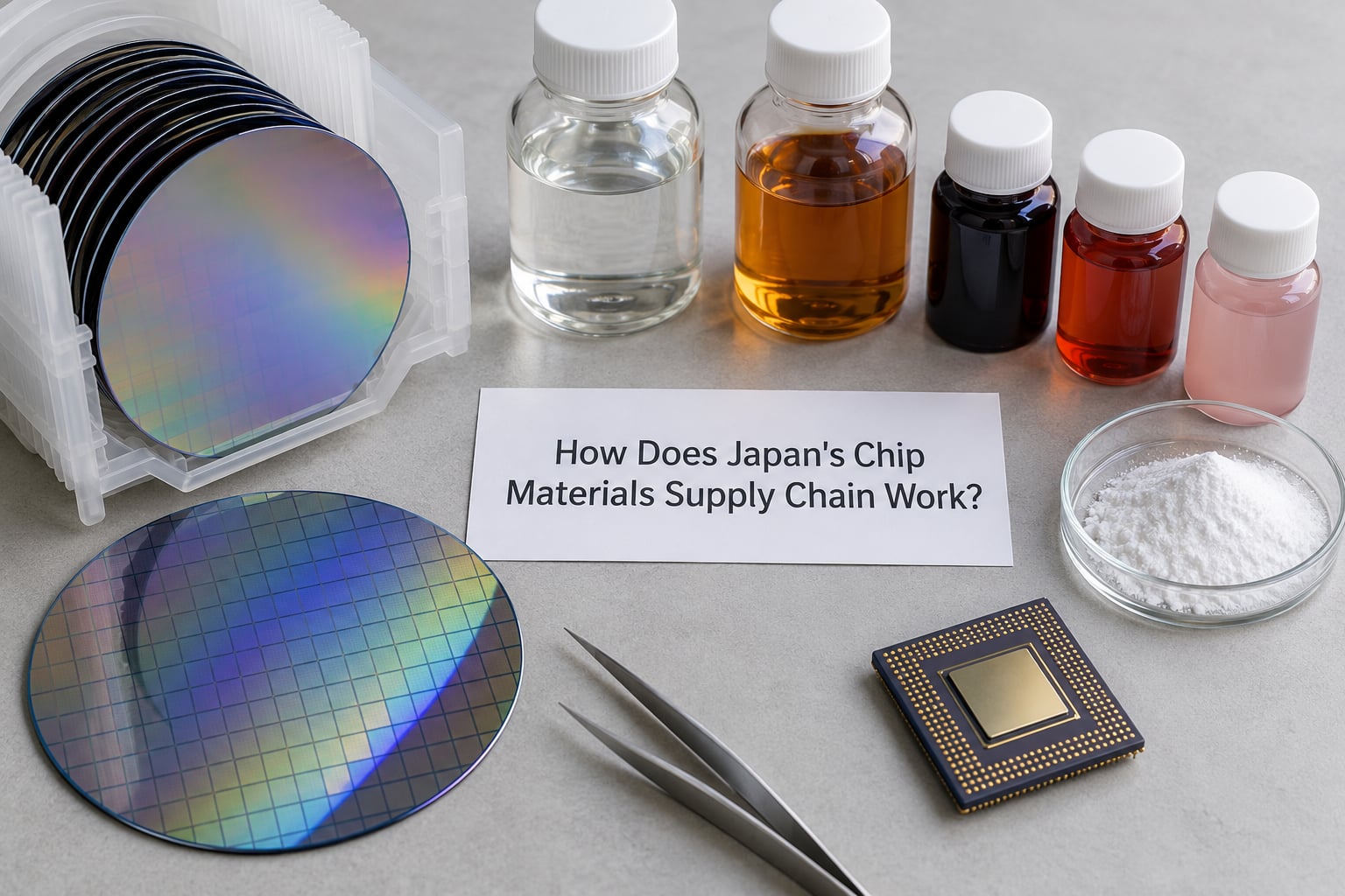
The chain has six layers, and Japan sits mostly in the middle two. Upstream are industrial inputs: quartz and industrial-grade silicon for wafers, petrochemical feedstocks for solvents and resins, and high-purity base chemicals. These are globally traded commodities with their own concentration problems.
Next come the specialist converters, which is where most of the Japanese industry lives. They purify, formulate, coat and package those inputs into fab-grade materials. Their competitive advantage is process knowledge accumulated over decades, not ownership of a raw material.
Then come the distributors. In Japan a familiar pattern is a converter producing at scale and a trading house or distributor handling delivery, documentation and inventory to the customer. A Western reader often misses this step and concludes that shipments are smaller than they are, because the material is counted once at the factory and not again on the truck.
Fab customers then qualify the material against a specific process, which is where the chain effectively locks. A chip designer specifies the process, the fab runs it, and a designer like a fab in Hsinchu can end up holding Japanese resists, Japanese masks and Japanese build-up film without anyone involved consciously deciding on Japan. The material arrived when the process was built.
End markets sit downstream: AI accelerators, high-bandwidth memory, smartphones, automotive control units and power devices. The reason a Japanese material shows up in a Taiwanese or American chip is simple. Fabs are the buyers, and Japanese suppliers won the specification for those process steps.
Which Japanese Companies and Regions Matter Most?
No rankings follow, because share estimates age badly and a list of the biggest companies would blur the point. These are representative names for each category, included so the segment makes sense.
Silicon wafers. Shin-Etsu and SUMCO are the two names that come up in any wafer discussion, with Shin-Etsu also a major force in PVC and silicones, which is a good illustration of how a materials conglomerate carries semiconductor divisions.
Photoresist and photomask materials. JSR, Tokyo Ohka Kogyo, Shin-Etsu and Fujifilm supply resists, while Hoya and a small set of specialists hold the mask blank and advanced mask categories. Fujifilm’s presence surprises people until you remember it was a photosensitive film business before it was anything to do with chips.
Specialty gases and wet chemicals. Air Water, Air Liquide Japan operations, Kanto Denka, Nippon Sanso and a cohort of wet chemical suppliers cover this band. It is the most contested category, with Chinese localisation advancing faster than in resists.
CMP and advanced materials. Resonac, Fujimi and Kanto Denka appear here, and Resonac has been publicly discussed as a consolidation target given its restructuring and its stated interest in further deals.
Packaging and films. Ajinomoto for ABF, Resonac and Shin-Etsu for mould compound and films, and Sumitomo Bakelite for advanced package resins. That last group is the least known and among the most concentrated.
Equipment that coats and processes. SCREEN and Tokyo Electron are not materials companies, but they belong in the same story. Tool makers and resist makers are developed and qualified together, which is part of why the pair is hard to separate in practice.
Geographically, plants cluster around a few industrial corridors. Yamaguchi Prefecture in the far southwest of Honshu has become a photoresist hub, with a workforce and supplier base built over decades around firms that expanded rather than started there. Tokyo and Kanagawa hold corporate and R&D functions, Shizuoka and Yamanashi have chemical and materials plants, and Kyushu carries a growing share of assembly and, increasingly, front-end capacity.
Why Is Japan Important Despite Limited Chip Fabrication?
Because the division of labour in semiconductors assigns different countries different layers. Front-end fabrication at the leading edge is dominated by a small number of enormous companies in Taiwan, South Korea and the United States. Each of those companies needs a material set of dozens of specialised inputs, and a supplier set short enough that a procurement team can qualify it properly.
Japan ended up in the supplier seat for a mundane reason: the domestic electronics industry of the 1970s and 1980s demanded materials that nobody else yet made at the required quality, and the companies that learned to make them kept the business when the assembly moved abroad. Materials capability outlived the factories it was originally built for.
Three things protect that position. The first is process know-how, which lives in formulation details that are rarely written down anywhere. The second is qualification, described next, which turns knowledge into a commercial moat. The third is breadth: no other country has as many material categories in commercial quantity at once, so a fab can source several layers from the same national ecosystem.
Global capacity keeps growing regardless of where the fab sits. New fabs in Japan and overseas, including announced projects in Kumamoto, Kitakyushu and beyond, need local or regional material supply, and a material supplier willing to build next to a customer is far easier to approve than one shipping across an ocean.
How Do Semiconductor Qualification and Quality Control Work?
Qualification is the mechanism that makes this industry work, and it is the least understood part. A materials supplier does not sell a product into a fab and hope. They supply sample batches, which the fab runs through a real process, often at the risk of scrap, and measure yield, defect rates, line-edge roughness, thickness uniformity and metal-ion content against the previous material.
The bar is not “good enough.” It is good enough across many process steps, at a defect rate low enough that a change does not quietly cost yield, with batch-to-batch consistency that holds over years. A supplier that clears that on one fab and one process has proven almost nothing, because resist, mask and slurry behaviour depends on the rest of the recipe.
Practitioners who work inside these lines point to the switching cost plainly: once a material is qualified, changing it risks scrapping entire wafer runs, and the new supplier has to clear the same test again. That is why fabs qualify multiple sources very reluctantly, and why a materials supplier that holds a slot can be remarkably durable.
Three practical consequences follow. First, share moves slowly in both directions, which cuts both ways for a competitor trying to break in. Second, documentation and traceability carry more weight than in many other industrial businesses, because a fab must be able to show which lot built which wafers. Third, price is rarely the deciding factor once a material is inside a working process, though it dominates conversations before qualification starts.
What Are the Main Risks to Japan’s Materials Industry?
Several of these are documented conditions rather than forecasts, and it is worth separating them from speculation.
Natural hazard and energy costs. Chemical plants sit in earthquake-prone parts of Japan, and several materials plants were affected by the 2011 earthquake and tsunami. Energy is the other side of the same coin: ultra-purification and high-temperature synthesis are electricity-hungry, and Japanese industrial power has remained expensive relative to many competitors.
Imported inputs. Japan is a large importer of industrial feedstocks and, in a chokepoint conversation, also of upstream gases and resins. Strength at the conversion step does not remove that exposure.
Workforce. The same demographic pressure that affects Japanese manufacturing generally applies here, and there is no large pool of process engineers to draw from.
Customer concentration. A concentrated customer base means a materials supplier’s revenue is tied to a handful of fab investment cycles, and it gives those customers real negotiating leverage.
Export controls and geopolitics. Japan has aligned its export control lists with allied regimes on advanced equipment and materials, and resist has been discussed publicly as a category that could be used as leverage. Nobody should treat that as a settled policy; treat it as a live possibility that has been articulated.
Competition. China is localising materials deliberately and has made visible progress in wet chemicals, targets and some gases, with a different playbook from Japan’s: state capital, abundant engineers and a large captive domestic market. South Korea and Taiwan are building on their own strengths, and Europe and the US each have targeted programmes intended to restore domestic capacity.
Solvents specifically. Semiconductor-grade PGME and PGMEA have drawn fresh attention as a pressure point, with reporting pointing to upstream feedstock constraints as a driver. This is the clearest recent example of a low-visibility chemical turning into a headline.
None of these are reasons to discount the industry. They are reasons to expect share to move in small steps over a decade rather than in a single quarter.
What Could Strengthen Japan’s Position in Chip Materials?
New front-end fabs in Japan are the most visible driver, because a fab built next to a materials supplier is a fab that can localise its inputs. Government subsidy programmes have supported both the fabs and the materials ecosystem around them, and the spillover effect on supplier investment is at least as important as the fab itself.
Public research and development funding matters here for a specific reason. The chemistry that matters most is chemistry that has not yielded a product yet. Programmes aimed at next-generation resists, mask materials, CMP chemistry and precursors fund the long tail that becomes next decade’s bottleneck.
Advanced packaging is the segment where growth looks most reliable, because chiplets and stacked memory increase the amount of substrate material per device regardless of which node anyone manufactures at. Japan’s film and compound suppliers sit directly in that path.
Equipment demand helps materials indirectly. When domestic tool makers win a generation of process tools, their chemistry partners are pulled into the same fabs, and a resist designed alongside a track has a practical advantage over one designed blind.
Workforce development is the least photogenic item and the one with the longest lead time. Every other improvement on this list eventually runs into the limit of how many people in the country can run a high-purity chemical line.
How Should Investors and Tech Professionals Read Industry News?
Most confusion in this sector comes from announcements that are about one layer being reported as though they are about another. Four checks help.
Identify the layer first. A company making coating and developing equipment is not a materials company, and a materials company is not a fab. A press release about new fab capacity says nothing about resist supply, and a press release about resist supply says nothing about wafer output.
Ask what kind of news it is. Capacity announcements are plans. Qualification announcements mean a customer has run a process. Investment announcements are money committed. Only shipment and revenue data show what actually happened, and the gap between those four is where most disappointment lives.
Check the vintage of the number. Share figures in this industry are typically two to five years old when they appear, because the underlying market studies are published slowly. If a page quotes 90% concentration for photoresist and gives no year, assume the number is older and directional.
Treat concentration as segment-specific. A company may dominate one material and be marginal in the next. The recurring pattern of the past year has been a headline about a Japanese monopoly in a category that turns out to be a sub-segment, with the neighbouring category already contested.
One more habit helps: check whether a claim is a company statement or an independent estimate. Company statements about their own position are promotional by default. That does not make them false, but it does make the framing worth noticing.
Frequently Asked Questions
Is Japan a major semiconductor manufacturing country?
Japan operates semiconductor fabs, including leading-edge projects, and has a long industrial history in devices. But it is not a major chip manufacturing centre by output. Large-scale fabrication is concentrated in Taiwan, South Korea, the United States, mainland China and Europe, where a handful of companies operate enormous fabs. Japan’s weight sits upstream, in the materials those fabs consume.
What chip materials is Japan best known for supplying?
Photoresist is the best known, with several published breakdowns putting Japanese suppliers at roughly 90% or more of global supply. Japan is also prominent in 300mm silicon wafers, advanced photomasks and mask blanks, electronic specialty gases, high-purity wet chemicals, CMP slurries, and build-up film for high-end packaging substrates, where the Ajinomoto ABF film is the standout example.
Does Japan manufacture the silicon used in its semiconductor materials?
Partly, and it matters that it does not fully. Japan converts imported or domestically produced ultra-high-purity polysilicon into ingots, wafers and finished wafer surfaces at a very high level, which is where its value sits. The purification of the raw polysilicon itself, and the production of industrial-grade silicon, is a separate and more internationally distributed step, so Japanese wafer makers remain exposed upstream.
How important are Japanese photoresists to chip production?
Very important, because resist is consumed at every lithography layer and is tightly matched to the process and the coating tool. A leading-edge logic or memory chip can pass through a fab process dozens of times, and each pass needs a resist that holds the required line width. Because a qualified resist is rarely swapped, concentration among Japanese suppliers has a practical effect on how fast global advanced chip output can change.
Can Japan reduce its dependence on imported semiconductor materials?
Partly, and the effort is under way. New fabs in Japan give materials suppliers a reason to build local plants close to customers, and subsidy programmes support both fab and materials investment. Dependence on imported petrochemical feedstocks, base chemicals and some gas feedstocks is harder to shift, because those inputs depend on global refining and chemical capacity. Expect partial progress over a decade rather than self-sufficiency.
Conclusion
Japan’s importance in chips is not about how many transistors it builds. It is about how much of the material those transistors are printed on leaves the country every week, and how long a qualified customer waits before replacing it. That combination of concentrated supply, invisible presence and slow substitution is the real story, and it is the opposite of the usual framing of a country that lost its chip industry.
If you want one starting point, pick the layer that interests you. Silicon wafers teach the physical substrate. Photoresists teach the process and the qualification lock. Advanced packaging materials, from ABF film onward, are where the newest money and the newest AI demand are landing, and where the least is written for general readers.
For anything published on this topic after October 2026, check the layer before you check the claim. The layer tells you whether the news means anything.