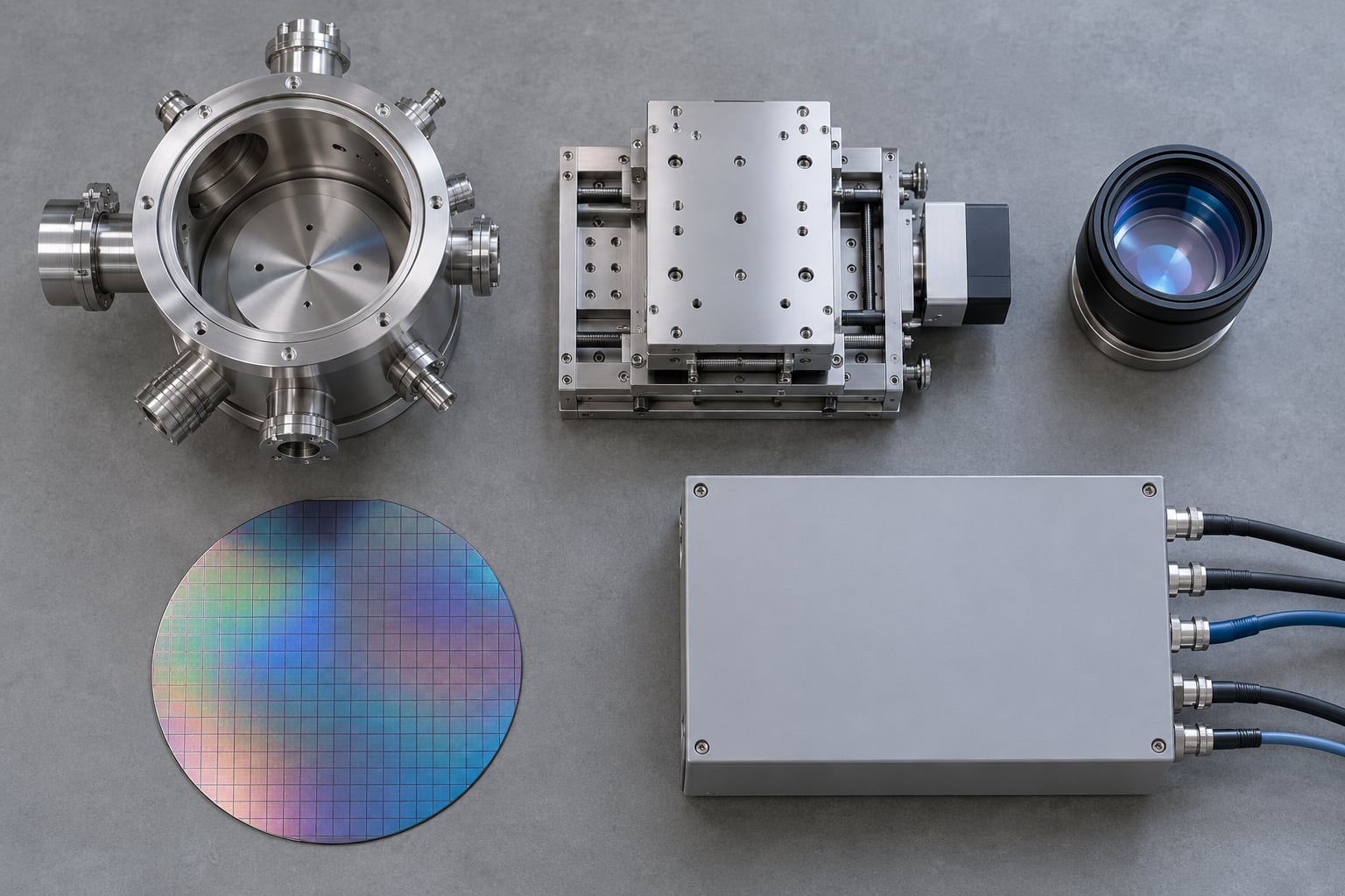
Japanese toolmakers do not try to outspend Applied Materials or Lam Research across every kind of chip equipment. They win by owning specific steps of the wafer process — coating and developing photoresist, etching, cleaning, thermal processing, testing, dicing — and then defending those steps with customization, a long-lived installed base, and field engineers who show up when a fab has a problem at three in the morning.
That approach is why Japan can hold a leading share of the world’s semiconductor production equipment while its share of global chip fabrication sits far lower. The tools travel; the fabs largely do not.
Table of Contents
- 1Why Japan’s Semiconductor Equipment Makers Matter
- 2How Semiconductor Equipment Makers in Japan Compete at a Glance
- 3Which Markets and Customers Do They Serve?
- 4How Do They Turn Process Expertise Into a Competitive Advantage?
- 5How Does R&D and Product Breadth Reinforce Their Position?
- 6How Semiconductor Equipment Makers in Japan Compete Beyond Hardware
- 7Why Do Scale, Service Networks, and Supply Chains Matter?
- 8How Do Export Reach and Japan’s Business Model Add Resilience?
- 9What Challenges Do Japanese Equipment Makers Face?
- 10How Can You Evaluate Their Competitive Strength?
- 11Frequently Asked Questions
- 12Who are the leading Japanese semiconductor equipment makers?
- 13Why are Japanese companies important in semiconductor manufacturing equipment?
- 14What is the biggest competitive advantage of a Japanese equipment maker?
- 15How important is maintenance and customer service in this industry?
- 16How do export controls affect Japanese semiconductor equipment companies?
- 17Conclusion
Why Japan’s Semiconductor Equipment Makers Matter
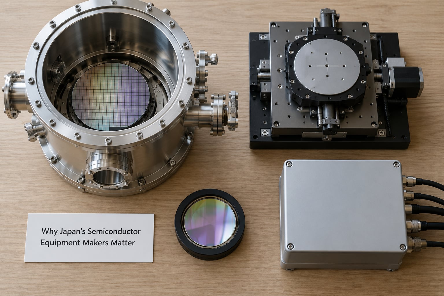
Japan’s equipment makers matter because they supply the machines that build every advanced chip, whoever builds it. The country’s tool sector holds a leading share of global semiconductor production equipment, second only to the United States overall, with several firms ranked first outright in their categories.
The equipment families they cover map onto the fab floor. Lithography from Nikon and Canon prints patterns onto wafers. Deposition and etch, led by Tokyo Electron, lay down and carve away the thin films that become transistors and interconnects. Cleaning, SCREEN Holdings’ core business, removes contamination between steps. Thermal processing, Kokusai Electric’s strength, heats wafers to drive reactions and diffusion. Inspection and metrology from Hitachi High-Tech measures what was built. Test from Advantest checks whether chips work, and dicing and grinding from DISCO separates the finished die.
Materials count too. Japanese suppliers hold dominant positions in photoresist and in high-purity silicon wafers, and those materials were designed around the tools that apply them.
How Semiconductor Equipment Makers in Japan Compete at a Glance
The levers below are not all equal at every company. Some firms lean on one, others on four at once. Reading the table as a profile rather than a ranking is the useful part.
| Competitive lever | What it actually means | Who leans on it hardest |
|---|---|---|
| Process-step leadership | Being the reference tool for one step so fabs qualify competitors against your benchmark | Tokyo Electron (coat/develop, etch), SCREEN (cleaning), DISCO (dicing) |
| Installed-base support | Selling maintenance, spares and upgrades for tools already in production | Every large maker, but deepest where uptime matters most |
| Customer collaboration | Building a tool with a specific fab and qualifying it together | Tokyo Electron, Kokusai Electric, Advantest |
| Product breadth | Several tools spanning a process flow, sold into the same account | Tokyo Electron, SCREEN Holdings, Hitachi High-Tech |
| Service coverage | Local application centres and field engineers near the customer’s fab | Advantest, DISCO, Tokyo Electron |
| Manufacturing scale | Enough capacity to deliver on a fab’s ramp schedule, and keep parts flowing for a decade | Tokyo Electron, Canon, Nikon, Hitachi High-Tech |
| Export reach | Sales and service subsidiaries in every region where wafers get made | All of them; SCREEN and Canon are most exposed to the shift in China demand |
Read together, the pattern is a loop rather than a list. A tool ships, the installed base grows, service revenue follows, and that revenue funds the next generation for the same process step.
Which Markets and Customers Do They Serve?
These companies sell to chip factories, not to end consumers. Their customers split into a handful of groups, and each group stresses a different part of the tool.
Leading-edge logic fabs need the tightest overlay and the fastest cycle times. Memory producers pushing 3D NAND and DRAM stack many identical layers, so throughput and thermal uniformity dominate. Foundries run many product families on shared lines and want predictable, repeatable recipes. Power and automotive chipmakers work in smaller fabs with long qualification cycles, where reliability outranks headline throughput. Advanced packaging operations, including those handling high-bandwidth memory and chiplets, need dicing, grinding and hybrid bonding tools. Research institutions buy pilot and development systems, often as the first reference for a technology.
The mapping of step to specialist is the clearest single answer to how these firms compete:
| Process step | Leading Japanese maker | What it sells |
|---|---|---|
| Coating and developing photoresist | Tokyo Electron | Tandem coater/developer tracks for lithography |
| Dry etch and deposition | Tokyo Electron | Single-wafer etch, CVD and ALD platforms |
| Wafer cleaning | SCREEN Holdings | Batch and single-wafer cleaning, plating |
| Batch thermal processing | Kokusai Electric | Furnaces for oxidation, anneal and diffusion |
| Automatic test equipment | Advantest | ATE systems and probe cards for logic and memory |
| Dicing and grinding | DISCO | Dicing saws, grinders, blades and wheels |
| Metrology and inspection | Hitachi High-Tech | CD-SEM and defect inspection |
| Photolithography | Nikon, Canon | DUV immersion and dry scanners for mature and specialty nodes |
| Vacuum and support | Ebara, Ulvac | Dry pumps, valves and load-lock components |
That is a portfolio of specialists, not one company with everything. It is a deliberate choice, and it is the biggest structural difference from the US full-line model.
How Do They Turn Process Expertise Into a Competitive Advantage?
The advantage comes from what the maker learns while a tool sits on a customer’s line, not from the tool’s spec sheet. A process engineer can measure chamber condition, particle counts and drift patterns on an installed system and feed them back into the next design.
Close collaboration pays off in four measurable ways. Yield improves when particle generation and contamination paths are engineered out rather than filtered out later. Process stability improves when a tool holds its conditions over weeks instead of hours. Throughput improves when handling time is designed around the process, not bolted on. And time to production shortens, because a fab buying a proven platform skips part of the qualification grind.
The hard part is that this knowledge is not written down in a datasheet. It accumulates in the heads of application engineers who have spent years inside customer fabs, and it is very hard for a newcomer to buy. A rival with a better laser and no field organisation often loses anyway.
How Does R&D and Product Breadth Reinforce Their Position?
Sustained research spending is what keeps a step leadership from being inherited rather than earned. Japanese toolmakers fund long-horizon programs on atomic layer deposition, plasma chemistry, stage precision and advanced packaging, and they protect the results with dense patent portfolios.
Breadth then does something research alone cannot: it spreads the cost. When a firm already has a customer relationship at a memory maker from its cleaning tools, adding an etch tool is cheaper than winning the account from zero. Several tools in one process flow also create a consistency argument — one vendor tuning deposition and etch together can promise results no single-tool supplier can.
As nodes shrink, this matters more. A customer migrating from one generation to the next needs vendors who already speak the new node’s process language, and incumbency carries most of that weight.
How Semiconductor Equipment Makers in Japan Compete Beyond Hardware
The sale is the easy half. The durable half is everything that keeps a qualified tool running for its fifteen-year production life: process recipes, spare parts, software upgrades, operator training, predictive maintenance and on-site engineering.
For a fab, changing a tool means requalification, which means yield risk and lost output. A supplier that already holds the process history is therefore not just convenient — it is safer. That is the lock-in mechanism, and it explains why service and parts revenue is a strategic asset rather than an afterthought.
Software is the quieter half of this. Control software that learns a tool’s normal behaviour and flags drift before a defect escapes can turn a maintenance visit from a breakdown into a scheduled adjustment. Few buyers evaluate this carefully, which means it is still a differentiator.
Why Do Scale, Service Networks, and Supply Chains Matter?
A fab does not shut down for maintenance, so response time is a purchasing criterion rather than a service detail. The big makers answer that with application centres near customer fabs, field engineers on call, and spare-parts inventories positioned close enough to matter.
Behind that sits disciplined manufacturing. These are contract manufacturers of specialist machines — vacuum chambers, precision stages, optical benches — and each depends on a small number of deeply qualified suppliers. Long-term supplier relationships, tight incoming inspection, and long-term component qualification are what let a decade-old tool still get correct parts.
Japanese quality management practice is often dismissed as a slogan, but in this industry it is a procurement requirement. Fabs audit suppliers, and audit failures cost more than a few percentage points of price.
How Do Export Reach and Japan’s Business Model Add Resilience?
Japan’s chipmaking share collapsed through the late 1980s and 1990s, and forum discussion of that period frequently points at the sharp yen appreciation that followed the 1985 Plaza Accord, which made domestic manufacturing uneconomic. Equipment share did not collapse with it. Tools sell to whoever is building chips, so Japanese suppliers followed the fabs to Korea, Taiwan, the United States, China and Southeast Asia.
The business model that follows from this is unusually portable. Overseas sales subsidiaries, local service operations and manufacturing outside Japan all reduce dependence on any one geography. Long customer relationships matter more than any one product cycle, and end markets spread across logic, memory, power, image sensors and packaging.
Government policy reinforces this. Japan’s multi-trillion-yen industry push backs domestic fabs — including the TSMC Kumamoto fabs and the Rapidus 2nm project — and those fabs become reference customers and development sites for domestic toolmakers. Whether subsidy or engineering drives the result is genuinely debated; the practical effect for suppliers is a domestic customer base to test tools in.
What Challenges Do Japanese Equipment Makers Face?
The position is strong but not comfortable, and the honest version names the pressure points.
US and EU rivals. Applied Materials and Lam Research compete with far larger budgets and broader product lines; ASML dominates the most advanced lithography outright, which effectively caps how far Nikon and Canon can compete at the leading edge.
Export controls. Washington and Tokyo both restrict advanced tool sales to China, and China has been a large share of several Japanese makers’ revenue. Compliance costs money and reshapes order books on short notice, which is why the stocks react sharply to control news.
Cyclicality. Equipment demand follows fab capital spending, which is volatile. A single weak year hits revenue hard regardless of how good the technology is.
The AI packaging gap. Advanced packaging, high-bandwidth memory and chiplet assembly have pulled value toward the companies that do bonding and integration, a field where Japanese participation is thinner than its front-end position would suggest.
Workforce. An ageing engineering population and a shortage of vacuum, optics and process specialists limit how fast headcount can scale with a ramp.
How Can You Evaluate Their Competitive Strength?
Assess any Japanese equipment maker on eight things, in this order. It takes about an hour with a company report and an industry association’s market breakdown.
Process leadership. Is the company the reference tool for a step, or a credible alternative in it? Repeat orders. Do the same fabs come back, or is every sale a first sale? Installed base. How many tools are in production, and how old are the oldest ones still supported? Service responsiveness. Where are application centres relative to the customer fabs? Customer concentration. How much revenue rests on one region or one customer type? R&D intensity. What share of revenue goes into research, and is it steady across a down cycle? Product breadth. Can the firm sell more than one tool into the same process flow? Regional manufacturing. How much production sits outside Japan, and does that create cost or resilience?
A firm strong on leadership, repeat orders and service but weak on breadth is a focused niche champion. A firm weak on service but strong on breadth is a full-line vendor competing on roadmap. Both are viable; they fail differently.
Frequently Asked Questions
Who are the leading Japanese semiconductor equipment makers?
Tokyo Electron leads in coat/develop and etch, SCREEN Holdings in wafer cleaning, Advantest in automatic test equipment and probe cards, DISCO in dicing and grinding, and Kokusai Electric in batch thermal processing. Hitachi High-Tech is strong in metrology and defect inspection, while Nikon and Canon supply DUV photolithography scanners. Ebara and Ulvac make the vacuum pumps and components other tools depend on.
Why are Japanese companies important in semiconductor manufacturing equipment?
Because a chip cannot be made without the tools. Japanese makers hold a leading share of global semiconductor production equipment, second only to the United States, and lead outright categories including wafer cleaning, dicing, batch furnaces and most coat/develop tracks. Their customers include leading-edge foundries, memory producers and power device fabs in Korea, Taiwan, the United States, China and Japan itself.
What is the biggest competitive advantage of a Japanese equipment maker?
Ownership of a specific process step, reinforced by the installed base behind it. Once a fab qualifies a tool, changing it means requalification, yield risk and lost output, so the supplier that already holds the process history is usually the safer choice. That makes service, spare parts and process collaboration a durable moat rather than an add-on, and it is what a new entrant has to overcome.
How important is maintenance and customer service in this industry?
Critical, because fabs run around the clock and cannot stop for a breakdown. Maintenance, spare parts, software upgrades, operator training and on-site engineering keep a fifteen-year-old tool qualified and running, and they generate recurring revenue that funds the next tool generation. That relationship is also why toolmakers build application centres and field teams close to customer fabs instead of exporting everything from Japan.
How do export controls affect Japanese semiconductor equipment companies?
They cut both ways. Restrictions on selling advanced tools to China reduce addressable demand and force compliance spending, and several makers depended heavily on that market. At the same time, controls push customers toward non-Chinese capacity, which favours Japanese suppliers with global service networks. The main effect is volatility: revenue forecasts shift quickly whenever rule changes are announced.
Conclusion
Japanese semiconductor equipment makers compete by going narrow on purpose. Each firm leads a process step, learns it deeply inside customer fabs, then defends it with an installed base that is expensive and risky to replace. That is a different game from the US full-line model, and it explains how the sector holds a leading global share of equipment while Japan’s share of chip fabrication sits much lower.
If you are assessing a specific company, look at five things first: whether it leads its process step outright, whether the same fabs order again, how large and how old the installed base is, how close the service teams sit to the customer’s fabs, and how much production sits outside Japan. Those five answers usually tell you more than a product roadmap slide does.